ISSN ONLINE(2278-8875) PRINT (2320-3765)
ISSN ONLINE(2278-8875) PRINT (2320-3765)
Shital S. Bramhe1, Milind S. Narlawar2, S. L. Badjate3
|
| Related article at Pubmed, Scholar Google |
Visit for more related articles at International Journal of Advanced Research in Electrical, Electronics and Instrumentation Engineering
The proposed microstrip-feed antenna mainly consists of circular monopole antenna (CMA) with defected ground structure for cognitive radio application is presented. The proposed antenna uses FR-4 substrate having thickness of 1.6mm and dielectric constant of 4.4. This antenna achieves an enhanced impedance bandwidth of 2.98GHz. Most of the work in cognitive radio domain has been done in the frequency range of 3.1GHz to 10 GHz, but this paper presents a CMA operating over frequency band of 0.6GHz to3.58GHz. The proposed antenna was designed and analyzed by using software HFSS (Higher frequency simulation software) 13.0 which is suitable for cognitive radio applications.
Keywords |
| cognitive radio, ultra wideband, defected ground structure, sensing antenna, reconfigurable antenna |
INTRODUCTION |
| The rapid growth of communication systems and the increase demand for frequency bands have caused a shortage in the available RF spectrum. Current spectrum allocations are highly underutilized where it is found that the spectrum can be idle for 90% of the time [8]. Cognitive radio system based on software defined architecture aims to improve the spectrum utilization by changing the transmitter parameters based on the interaction with the environment in which it operates [8].For cognitive radio application, both, a Wideband antenna for channel sensing and a reconfigurable antenna for communication are required. |
| The concept of reconfigurable antenna refers to a change in the frequency characteristics, radiation pattern, impedance bandwidth and polarization of an antenna by changing its aperture dimensions or geometry through electrical or mechanical means. An antenna with reconfigurable frequency response can either switch abruptly from one frequency band to another or continuously perform this task. The frequency response reconfigurability is achieved by actively controlling the effective electrical length of the antenna thus enabling the antenna to operate in different frequency bands. This is usually done by adding or removing a part or parts of the antenna through electrical, mechanical, optical, or other means. |
| Defected patch structure (slit or slot in patch) is used to reduce size of antenna. Defected patch structure is realized by etching the conducting patch and defected ground structure is realized by etching the conducting ground plane of microstrip antenna. This disturbs the shield current distribution in the plane which influences the input impedance and current flow of the antenna. The geometry of defected patch structure can be one or few etched structure, which is simpler and does not need a large area to implement it. |
| Antenna at different resonances, reveal their dependence on the antenna dimensions and shapes. Cognitive radio antenna integrated with DMS-BSF and inverted π shaped slot has been designed to achieve notch band characteristic [1]. L-shaped and staircase defect on left side and staircase defect with bend on right side ground plane antenna has been used to achieve two resonant modes with excellent impedance performance [2]. |
| Spider Microstrip Antenna with New Defected Ground Structure. DGS shapes achieve a size reduction about 41% compared to dumbbell shape [4]. |
| Two separate antennas are suggested with one directional for communications and the other omni-directional for sensing. Single antenna cognitive radio platforms have also been proposed. The antenna used both for sensing and communication.[1] Frequency agile functionality is achieved using a tunable filter.[6] Instead of multiple antennas or a single wideband antenna, reconfigurable antennas are likely to be useful by combining wide and narrowband functionality and also allowing some additional pre-filtering, which are now considered to be potentially vital to successful cognitive radio operation [1].A triple-band monopole antenna suitable for WLAN applications is proposed.[2] An ultra-wideband printed monopole antenna with dual band-notched characteristics is designed for avoiding interference with Worldwide Interoperability for Microwave Access ( Wi-Max) (3.4 -3.69 GHz) and Wireless Local Area Networks (WLAN) (5.15- 5.825 GHz).[3] The proposed antenna is operated in the S-band and X-band with three resonant frequencies. The antenna has two resonance in the X-band used in Satellite communications other in the S-band at 4.98GHz frequency [5]. |
DESIGN PROCEDURE OF ANTENNA |
| The proposed circular monopole antenna is shown in Fig. 1, and the design parameters were calculated using the following steps: |
| A. Radius of patch (A) |
| According to, the size of CMA can be calculated via the following equations [6]: |
 |
| Where fL=800MHz is the lower band-edge frequency, P is the length of the 50Ω feed line in cm, which has been optimized for this design to 1.8mm , and the approximated value of εeff is given by[6]: |
 |
| For FR4 substrate with thickness of 1.6 mm εeff =2.7. L is length of CMA respectively. Using equation (1) with P=1.8mm, fL=800MHz we estimated A=4cm.To keep margin in fL, radius is chosen as 4.5cm (45mm). |
| B. Microstrip Line Width (WStrL) |
| The microstrip line width has been calculated from the following equation [10] |
 |
| Where Z0 is the characteristic impedance of the microstrip line, h is the substrate thickness which has been taken 1.6mm as a typical value, t is the metallization thickness which is 0.035mm, Wstrl is the microstrip feed line width and εr for FR4 substrate is 4.4. Therefore according to equation (4), for the characteristic impedance of 50Ω. Wstrl must be equal to 3mm. |
| C. Ground Plane Length ( Lg )[6] |
 |
| fL= 800MHz , εeff =2.7, we calculated value Lg which is approximately equal to 50mm.The radiated patch occupied a total volume of 110 × 160 ×1.6 mm. |
GEOMETRY OF AN ANTENNA AND SIMULATION RESULTS |
| A. Geometry of Circular Monopole Antenna and Simulation Results |
| The proposed circular monopole antenna can be designed by using partial ground plane which is shown in Fig.1. The circular monopole antenna with radius 45 mm, a 50 Ω microstrip feed line are printed on one side of the FR4 substrate. The length and the width of the dielectric substrate are 160x110 mm. The width of the microstrip feed line is fixed at 3mm to achieve 50Ω impedance. |
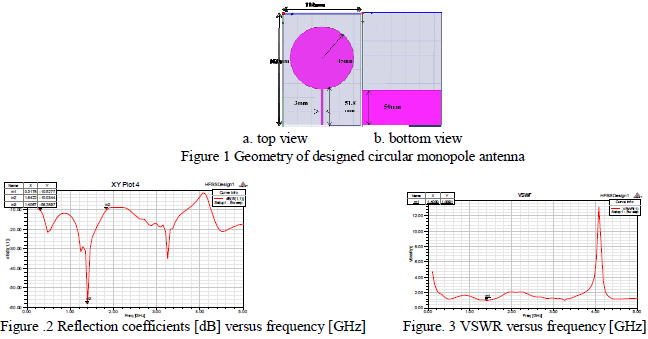 |
| From the simulated result, a wide impedance bandwidth of about 1.53 GHz (0.31-1.84 GHz) has been achieved. Minimum return loss is equal to -58.58db at resonance frequency of 1.40GHz and vswr equal to 1.0091 which is shown in fig 3. |
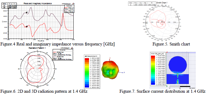 |
| 50.42 ohm impedance and 0.1422 mho reactance has achieved at resonance frequency 1.4GHz which nearly equal to expected values 50ohm and 0mho respectively.. 3D pattern is approximately omnidirectional and 2D pattern shows vertical pattern i.e 8 shaped at theta =90 degree , phi=90 degree and horizontal pattern at theta =90 degree , phi=90 degree. |
| B. Size Reduction of Patch Using Slit |
| By incorporating slit in patch we can reduced the patch size to some extent and broad bandwidth can be achieved. If slit is added on upper side of patch then there is no substantial change in radiation pattern as minimum surface current distribution is present on upper side of patch. |
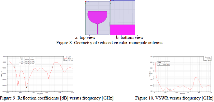 |
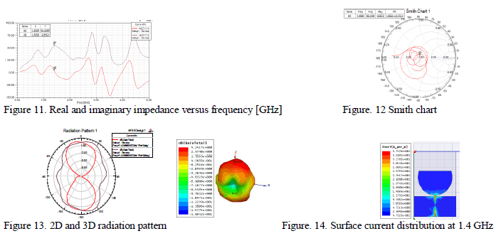
| CMA operates in the frequency range of 0.31GHz to 1.84 GHz i.e bandwidth is equal to 1.53GHz. By incorporating slit in patch bandwidth can be increases to 2.87GHz. |
 |
| C. Geometry of Circular Monopole Antenna with Slit and Dgs |
| Defected patch structure (slit or slot in patch) is used to reduce size of antenna. Defected patch structure is realized by etching the conducting patch and defected ground structure is realized by etching the conducting ground plane of microstrip antenna. This disturbs the shield current distribution in the plane which influences the input impedance and current flow of the antenna. The geometry of defected patch structure can be one or few etched structure, which is simpler and does not need a large area to implement it. |
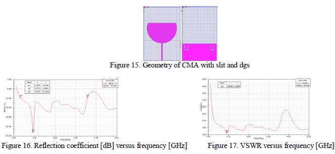 |
| The VSWR plot shows the impedance bandwidth from 0.32GHz to 3.57GHz and the lowest value of VSWR is found to be 1.10 at the frequency of 0.9GHz .The impedance bandwidth is calculated by considering VSWR in between 1 to 2. Impedance plot shows that the impedance value 54.43 at 0.9 GHz which is close to 50Ω. An antenna behaves as an ultra wideband sensing antenna which works in the frequency range of 0.32GHz to 3.57GHz. Thus the antenna shows a wide bandwidth of about 3.25GHz .The impedance bandwidth is calculated by considering the range of frequencies below -10dB.The maximum return loss for the antenna is found to be -28.2dB at 0.9 GHz. The gain of the antenna is found to be 1.469e+001dB and the 3D radiation pattern shows almost Omni-directional radiation pattern and 2D radiation pattern shows a pattern of eight in E plane while it shows almost circular pattern in H plane. |
 |
| The impedance bandwidth is calculated by considering the range of frequencies below -10dB.The maximum return loss for the antenna is found to be -28.2dB at 0.9 GHz |
 |
| The gain of the antenna is found to be 1.469e+001dB and the 3D radiation pattern shows almost Omni-directional radiation pattern and 2D radiation pattern shows a pattern of eight in E plane while it shows almost circular pattern in H plane. |
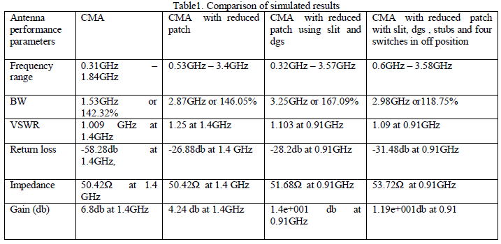
| Table 1 shows comparison of antenna at different stages . At every stage bandwidth will goes on increasing compared to previous one and other parameters are within the standard range. |
 |
| D. Geometry of Circular Monopole Antenna with Slit, Dgs, Four Stubs and Switches |
| This antenna is further modified by connecting stubs with the switches. By appropriate combination of switches the antenna works as a reconfigurable antenna. The geometry is further modified by addition of switches. The reconfigurable antenna with four switches s1, s2, s3, s4 shown in fig 22. By operating the switches in different on/off positions, the responses are studied and their combined response is also shown fig 24. It clearly indicates that with change in on/off position of switches, the operating frequency range of antenna changes |
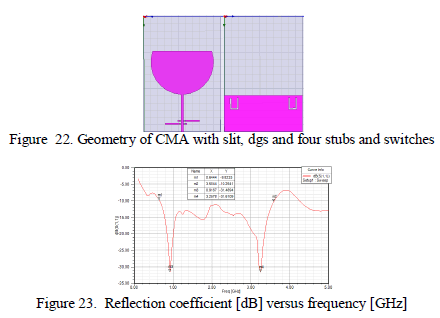 |
| From the simulated result, a wide impedance bandwidth from 0.644 to 3.58GHz has been achieved. |
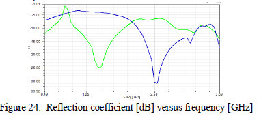 In fig 24 green colour indicate switch s1 and s4 are on s2 s3 are off. For this case bandwidth ranges from1.08 to1.95 GHzi.e0.87GHz. Antenna performance parameter like return loss , VSWR, gain, impedance came out to be -25db, 1.12, 5.19db,45.13ohm at 1.5GHz.Blue colour indicate s1off, s2 s3 s4 are on.For this case bandwidth ranges from (2.16 to3.31) GHz i.e 1.15GHz. Antenna performance parameter like return loss VSWR , gain impedance came out to be - 31db,1.05, 6.7db, 49.53 ohm at 2.55GHz. In fig 24 green colour indicate switch s1 and s4 are on s2 s3 are off. For this case bandwidth ranges from1.08 to1.95 GHzi.e0.87GHz. Antenna performance parameter like return loss , VSWR, gain, impedance came out to be -25db, 1.12, 5.19db,45.13ohm at 1.5GHz.Blue colour indicate s1off, s2 s3 s4 are on.For this case bandwidth ranges from (2.16 to3.31) GHz i.e 1.15GHz. Antenna performance parameter like return loss VSWR , gain impedance came out to be - 31db,1.05, 6.7db, 49.53 ohm at 2.55GHz. |
 |
CONCLUSION AND FUTURE SCOPE |
| The antenna can be used in a cognitive radio application for sensing and communicating purposes. The reconfigurable functions are obtained using four switches. By switching ON and OFF status of the four switches, antenna can work in four cases for underlay mode applications. As a result, they can well meet the WB cognitive radio requirement and effectively change the modes to prevent potential interference between secondary user and primary users. In the future, we will investigate the real switches, such as PIN diodes or switch circuit networks. |
| In the future, other reconfiguration techniques can be used such as electrical, mechanical. Fabrication of antenna can be done with PIN diodes, varactor diode, MEMS switches, photoconductive switches etc. |
| One can also discuss the implementation of an automatic antenna tuning unit system (ATU) for software-defined and cognitive radio. In order to meet the needs of the fast developing wireless and mobile services, further design and optimization of the ATU antenna system may be required to ensure high efficiency (low loss), low-power consumption, low profile, high speed tuning, and spurious free radiation in a particular application. |
References |
|