ISSN ONLINE(2278-8875) PRINT (2320-3765)
ISSN ONLINE(2278-8875) PRINT (2320-3765)
Nida-ul-Amin1, Hadia Amin2, Syed Sayir Farooq3, H. Najeeb-ud-Din4 (SM IEEE)
|
| Related article at Pubmed, Scholar Google |
Visit for more related articles at International Journal of Advanced Research in Electrical, Electronics and Instrumentation Engineering
With recent fast growth in the RF (Radio-Frequency) wireless communications market, the demand for high performance but low cost RF solutions is rising. Recent advances in SOI (Silicon on Insulator) and complementary metal oxide semiconductor (CMOS) processing, continuous scaling of gate length, and progress in silicon on insulator have stirred serious discussions on the suitability of metal-oxide semiconductor field-effect transistors (MOSFETs) for RF/microwave applications. The scale down of CMOS-SOI technologies has challenged toward the deep-submicron minimum feature size. This leads to great expectations for CMOS RF applications. This paper covers the recent advances and current status of mainstream CMOS and SOI as the dominating technologies in very large scale integration, future trends of RF MOSFETs, and applications of MOSFETs in RF electronics.
Keywords |
| CMOS, SOI, RF, MOSFET, LDMOSFET, VLSI. |
INTRODUCTION |
| In recent years, the interest in wireless communication and in the devices which can support such communication has grown rapidly. New wireless standards are being proposed every year. The targets for the manufacturers of wireless communication equipment are better radiation power, far effective distance, and large coverage range. The main driving forces behind the evolution of mobile terminals from a customer’s point of view are new application, miniaturization, increased and improved functionality and lower cost. With the development of a highly information oriented society, the RF (Radio-Frequency) wireless communications market has drastically grown up. In future, the demand of RF wireless technology will continue to increase all the more in various areas, e.g. our daily life, industries and medicine. This demand is met by the development of semiconductor products. Integration and power consumption reduction of the digital part will improve more with the continued downscaling of technologies [1]. Today, the transistor gate length in production is approximately 28nm. Further geometric scaling of conventional silicon MOSFET devices faces many fundamental challenges, such as: excessive gate leakage current, exponentially increasing source to drain subthreshold leakage current [2]. These problems can be solved with high dielectric constant materials, high-k, for gate oxide. |
| Following this introduction in this paper next we present the detailed history of RF CMOS and SOI technology, along with advanced MOS transistors for microwave and RF applications. Also we include the scope and future trends of RF MOSFETs, combination of MOSFETs with SiGe heterojunction bipolar transistors (HBTs, SiGe BiCMOS), and applications of MOSFETs in RF electronics. |
RELATED WORK |
| From extremely thorough review of related work and published literature, it is observed that many researchers have done rigorous work on the sustainability of mainstream CMOS as the dominating technology in very large scale integration. It is observed from the careful study of reported work that in the real world today VLSI/CMOS is very much in demand. |
| A review of advanced and beyond CMOS FET technologies for RF circuit design is represented by Ellinger et al. in his paper. The opportunities, limits and challenges for future silicon-based field effect transistors tailored for RF and millimetre wave circuit design are discussed. Also CMOS FET scaling, advanced CMOS techniques such as silicon on insulator, strained silicon, high-k, low temperature and multigate transistors are treated. Moreover, emerging beyond CMOS FET concepts based on silicon nanowires, graphene and carbon nano tubes are discussed as potential replacement or extension to CMOS. Liou et al. in his paper discusses recent advances in CMOS processing, continuous scaling of gate length, and progress in silicon on insulator technology. Despite some lingering debates, the prospects for RF MOS with operating frequencies in the GHz range are very promising. |
CMOS AND SOI TECHNOLOGY |
| The increasing demands on portable computing and communication devices have motivated the development of low-power radio frequency integrated circuits (RFICs). The low-voltage design is an effective method to decrease power consumption. Nowadays, CMOS technology has become a manufacturing choice for RFICs, due to its lower cost and higher integration capability. CMOS devices can be used in both analog and digital applications, making CMOS a suitable choice for mixed signal (analog and digital) circuits. High current driveability and small capacitances have been achieved by scaling down the physical dimensions of MOSFETs. Table 1 shows the history of RF CMOS. It has become possible for scaled MOSFETs to handle GHz-band RF signals. This advanced performance of CMOS is attractive for RF circuit design in view of a system on- chip realization. Since RF characteristics, such as the cut-off frequency (fT) and the maximum oscillation frequency (fMAX), of Si ULSI come to advance up to several tens of GHz [3]. Semiconductors used for RF CMOS may be III-V compounds based on GaAs and InP Si and SiGe or Wide band gap materials (SiC and III-nitrides). But there remain several issues in the design of CMOS for RF applications such as optimization of process conditions and difficulty with use of high resistive substrate. Also single chip solution results in coupling of the noise generated in different blocks of the transceiver system through the substrate. This problem can be overcome to a large extent by the use of SOI based devices [4]. |
| Table 1. History of RF CMOS [3] |
 |
| The Silicon-on-Insulator (SOI) CMOS technology has become a competitive technology for radio transceiver implementation of various wireless communication systems mainly due to low-power, low-cost, higher level of integrability, high performance mixed-mode circuits, etc [5]. SOI devices and circuits exhibit superior performance because of radiation hardness, high temperature operation, improved transconductance, sharper subthreshold, higher subthreshold voltage swing, excellent short channel behaviour. It has also improved speed, less power dissipation, and manufacturing compatibility with bulk silicon MOSFET technology. |
| Scaling down of the device to nanometer leads to some deteriorating effects: leakage current is increasing and second order effects like DIBL, SCE, are more apparent [6]. To get better performance, ultra thin body– UTB silicon film is generally adopted for the present nano-scaled conventional floating body SOI devices. UTB silicon film can suppress second-order effects to some extent. |
| However, there are problems associated with SOI: floating body effects viz kink and parasitic bipolar junction transistor, reduced breakdown voltage and self heating of the transistors. An upcoming promising technology which can be used to overcome the disadvantages of SOI like floating body effects and selfheating and works well at even low voltages is Dynamic Threshold Metal Oxide Semiconductor (DTMOS). DTMOS has very low leakages and this translates into low power consumption within the device. SOI technology is attractive for dynamic threshold MOS (DTMOS) [7] operation due to the absence of substrate loading and substrate coupling problems that are encountered in the bulk DTMOS devices. |
RF MOSFETs |
| In recent years the RF community started to notice the potentialities of MOS devices and many efforts started to appear in order to optimize the RF performance of the MOSFETs. Due to the channel length reduction, the cut-off frequencies of the MOSFETs have grown enormously in such a way that deepsubmicron devices start to present values higher than 400 GHz [8]. While strained silicon and high-k/metal gate technologies will continue to play significant roles in advancing present CMOS technology, the need for further scaling of the transistors will require the transistor structure as non-planar three dimensional (3D) structures such as the tri-gate transistors. An important measure of RF transistor is the cut-off frequency fT. This is the frequency at which the small signal current gain h21 of the transistor rolls off to unity (i.e., 0 dB) [9]. For 50 to 100 nm gate-length MOSFETs, the cut-off frequency has reached an astonishing value of 200 GHz [10, 11]. Applying a frequently used rule of thumb that the cut-off frequency should be around 10 times the transistor’s operating frequency, one could use these devices to design integrated circuits operating up to 20 GHz, an operating frequency higher than that for the great majority of modern RF electronics. Other figures of merit have to be considered as well. For example, a high maximum frequency of oscillation fMAX which is the frequency at which the transistor’s unilateral power gain rolls off to unity (i.e., 0 dB), is often desirable. Other desired aspects for RF MOSFETS like Pout, PAE (Power Added Efficiency), and MAG (Maximum Available Power Gain) should be as high as possible, Noise figure NFmin should be as low as possible but is always larger than 0 dB in real transistors. Besides all these requirements cost and reliability are also important factors in selecting RF devices. |
| Properly designed III–V RF field-effect transistors (MESFET and HEMT) show comparable fMAX and fT, but typically with fMAX > fT. The situation is different for Si MOSFETs. For these devices, one could either realize short-channel transistors for high fT but substantially lower fMAX or long-channel transistors for rather low fT but higher fMAX. This trade-off resulted from the fact that a very high fMAX can only be achieved with transistors having a high fT and a low gate resistance RG. For III–V FETs, metal gates with multi-finger mushroom structures are frequently used to minimize RG. The gates of Si MOSFETs are made of polysilicon, which has a much higher resistivity than a metal. Furthermore, for MOSFETs in digital applications, multi-finger and mushroom gates are not common. Reducing RG is imperative for RF MOSFETs because RG not only limits the power gain attainable at a certain frequency (and thus fMAX), but also sets a lower limit to the minimum noise figure. There are several means to minimize the gate resistance of Si MOSFETs like deposition of silicides on top of the polysilicon gate, metal over gates on top of the polysilicon gates, and multi-finger gates with small finger width [12]. |
| Recently we have 50-nm SOI MOSFET with an fMAX of 193 GHz (fT 178 GHz) and the 80 nm SOIMOSFET with fMAX of 185 GHz and fT of 120 GHz [3]. GaAs MESFET, AlGaAs HEMT give moderate output power densities and power amplification up to 60 GHz. pHEMT on GaAs, InP HEMT give moderate output power densities and Power amplification up to 100 GHz. whereas wide band gap FETs AlGaN/GaN HEMT, SiC MESFET gives highest output power densities up to 20 GHz. Wide band gap FETs show the highest output power densities of all RF FETs in the frequency range important for current mobile communication systems (up to 5GHz). |
A. LDMOSFET |
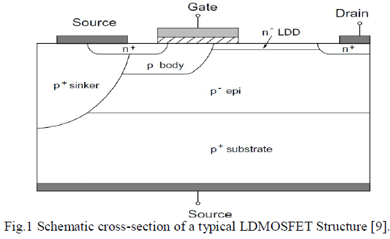
| High-power microwave amplifiers used in the base stations for mobile communication systems, are designed for maximum operating (and thus breakdown) voltage to deliver maximum output power. For such applications, a different MOSFET structure called the LDMOSFET (laterally-diffused MOSFET) is frequently used [9, 12]. The cross-section of a typical high-power LDMOSFET is shown in Fig. 1. It consists of a p+ Si substrate on top of a lightly doped p- layer grown epitaxially. While the n+ source region extends to the gate, the n+ drain region is spatially separated from the gate. The conductive connection between the n+ drain and the channel region underneath the gate is realized by an n- LDD (lightly doped drain) region which is frequently called the drift region. This is the main region contributing to a high breakdown voltage. Typically, the gate length of LDMOSFETs is in the range of 0.3–1.0 μm and the gate oxide is several ten nm thick. As such, the technology, especially the lithography and the gate oxide deposition, of the LDMOSFET is much more relaxed than that of the small signal microwave MOSFET. Depending on the specific designs, typical fT of LDMOSFETs is around 5–15 GHz, and the drain-to-source breakdown voltage is around 20–40 V. |
 |
| Concept of stacked lightly doped drain (LDD) has been used in silicon RF lateral double-diffused metal oxide semiconductor field effect transistor structure. The stacked layers of LDD minimizes the on-state resistance of the transistor due to the n+ doping used in the top LDD layer, and also raises the device breakdown voltage due to the charge compensation in the composite LDD region. Therefore, for the same blocking voltage rating, the stacked LDD structure allows the LDMOSFET to have a higher current handling capability. This in turn causes the transconductance to be higher, leading to higher RF performance for the power device [13]. |
APPLICATIONS OF CMOS AND SOI IN RF ELECTRONICS |
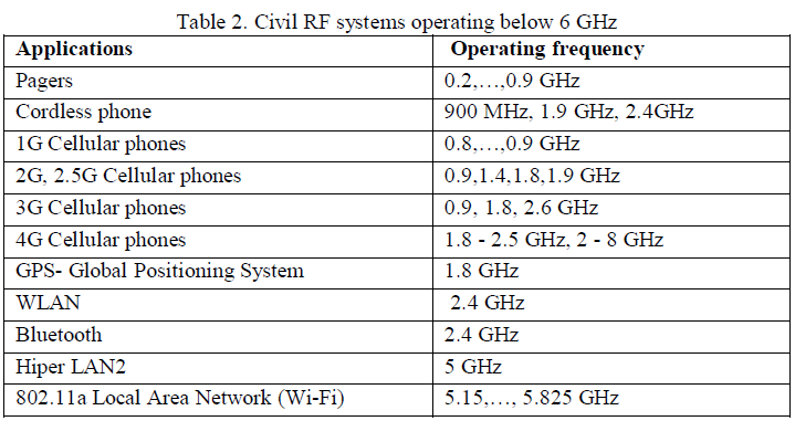
| The main stream of radio frequency (RF) applications is usually implemented in GaAs or silicon bipolar technology. On the other hand, during the last years, advances in complementary metal-oxidesemiconductor (CMOS) process technologies have continued to reduce the minimum channel length of metal-oxide-semiconductor field effect transistors (MOSFETs), thereby increasing the cut-of frequency (fT) of the devices [14]. Because of these relatively high fT values, bulk-silicon CMOS device is becoming viable technology choice in analog and RF applications for portable wireless communication systems. The operating frequencies of civil RF applications can range from a few hundreds of MHz to 100 GHz, but most systems having mass markets are operated at frequencies below 6 GHz. The number of units sold in these markets is in the order of millions per year. Table 2 summarizes various applications and their frequency spectrums [12]. Examples for civil communications systems in the higher frequency range are the Hiperlink system (17GHz), direct-to-satellite communication (20GHz downlink to 30GHz uplink), local multi-point communication services (27.5–29.5 GHz), millimeter-wave digital radio systems (23 and 38 GHz, and possibly 12, 15, 18, 26 GHz). Another field of civil microwave applications is automobiles. |
 |
| The envisaged applications include the global positioning system (1.8 GHz), collision avoidance radar (operating at 77 GHz), vehicle identification, traffic management, and others. Certain radar and sensor applications will operate around 94 GHz. At this time the principle handheld application is cell phones which require relatively small power devices that deliver several watts of RF power from a battery power source of a few volts. Such a system can be divided into the user part (handset) and the infrastructure part (base stations). The user part consists of a receiver and a transmitter. In the receiver part of a handset, lownoise RF transistors are used to amplify the incoming signals. As in any low-noise amplifier, the use of low minimum noise figure transistors is desired. GaAs MESFETs and Si bipolar transistors are the traditional low-noise transistors used in wireless communications, but the use of MOSFETs, possibly merged with SiGe HBTs using a low-cost BiCMOS process, has become a realistic option. |
| Low power consumption is particularly important in mobile communications due to limited battery life. One approach to meeting this challenge is to create a reduced power RF system-on-chip that contains digital, analog and RF portions of the design on the same die. SOI CMOS meets these requirements due to its reduced parasitic capacitance. The presence of the buried oxide layer not only reduces the junction capacitance but also offers the flexibility of using a high resistivity substrate to reduce the substrate-related RF loss. Microstrip losses as low as 0.03 dB/mm have been realized on high resistivity substrates at 2 GHz compared with 0.1 dB/mm on standard substrates [5]. In addition, improved passive device performance (resistor, capacitor and inductor) over frequency has also been demonstrated on SOI substrates. Another key concern with highly integrated RF/mixed mode circuit design is how to eliminate the cross-talk between high frequency RF and digital, mixed signal devices on the same die. This can be drastically reduced by using fully oxide-isolated SOI CMOS technology [5]. Complete oxide isolation of the active devices from the substrate eliminates the substrate current injection path. |
| One RF application is battery-operated, single-chip typical wireless transceiver [15]. The top priority for such a device is low power dissipation, which can be achieved by reducing the supply voltage. Dynamic Threshold-Voltage MOS (DTMOS) [7] can be considered the most suitable candidate for such applications. This is because the body of a DTMOS is tied to its gate, which can lead to an extremely high transconductance (gm) under very low supply voltages, and because DTMOS is built on an SOI wafer, which can reduce parasitic capacitance [16]. SOI-DTMOS is very promising to achieve high performance and at the same time avoid the strict requirements of technology and maintain the compatibility with conventional technology. At present, many researches indicate that micro-scaled and even nano-scaled SOI-DTMOS has much better performances than conventional SOI. SOI-DTMOS at nano scaled gate lengths, with excellent performances of both high speed and low power, is able to relax the critical requirement of silicon film thickness that strictly limits the application of conventional floating body SOI. SOI DTMOS can be used for very low power portable telecommunication systems. Lowering the supply voltage makes DTMOS a good candidate for remote control systems [17]. This evolution towards very low supply voltages for high frequency applications is only possible with DTMOS. |
| The dominant power RF transistor used in base stations of wireless communication systems with operating frequencies up to 2.5 GHz is the Si LDMOSFET, which in the last several years has replaced all other competing Si and GaAs transistors [12]. Si LDMOSFETs combine the advantages of moderate cost, high reliability and extremely high output power. Aside from cellular phones, several other civil RF systems with operating frequencies below 20 GHz are potential fields for the application of RF MOSFETs as well. For other applications below 20 GHz but with more stringent requirements concerning RF performance, the combination of SiGe HBTs and CMOS (SiGe BiCMOS) is currently a heavily discussed possibility in industry [55,56]. SiGe HBT will help to expand the market share of MOSFETs in RF electronics. SiGe HBTs offer excellent RF properties like high speed, i.e. both high fT and fMAX and low noise figure. |
| The emergence of commercial SiGe BiCMOS technologies with SiGe HBT fT and fMAX frequencies exceeding 170 GHz [18] illustrates the real possibility of the use of silicon HBT technology for millimetre wave applications. 60-GHz radio receiver blocks were recently demonstrated in a 0.13 μm SiGe HBT technology with impressive performance. SiGe HBT VCOs have demonstrated excellent output power and phase noise at millimetre wave frequencies [5, 18]. A silicon-based millimetre wave technology has the potential to realize the low-cost goals required to reach volumes for these next generation systems. A wide variety of semiconductor devices can meet the requirements for output stage power devices in GSM, DCS, CDMA, and WCDMA handheld applications. However there are some important tradeoffs among these devices. The higher power density of HBT’s leads to smaller die size. GaAs FET’s have higher power gain and PAE. Si LDMOS FET’s have the lowest cost even though they have the lowest power density and therefore, the largest die size [19]. Cell phone infrastructure base stations are the largest market for high power RF semiconductor devices. In general, these relatively large devices deliver tens or hundreds of watts from tens of volts. At this time Si LDMOS FET’s are the most widely used technology for this application. In recent years, very high power GaAs MESFET’s and pHEMT’s have been shown to have superior performance compared to Si LDMOS devices especially at higher frequencies. However, the cost of these GaAs FET’s is several times that of the Si devices even though much of the device cost is in the cost of the package. Today the infrastructure RF power device market is dominated by Si LDMOS with GaAs devices finding increased usage above 2 GHz [19]. |
| SOI laterally diffused MOSFET that is designed for use in radio frequency power amplifiers for wireless system-on-a-chip applications has been fabricated. Implementation of a LDMOSFET in thin-film SOI enables power amplifiers with improved gain, efficiency and bandwidth [20]. Moreover, implementation of a LDMOSFET in thin-film SOI may allow the integration of the RF power amplifier (PA) into a wireless system-on-a-chip, in which all of the digital, analog, and RF circuits of a wireless system are integrated on to a single die. The device is fabricated on a thin-film SOI wafer using a process that is suitable for integration with SOI CMOS. |
FUTURE TRENDS |
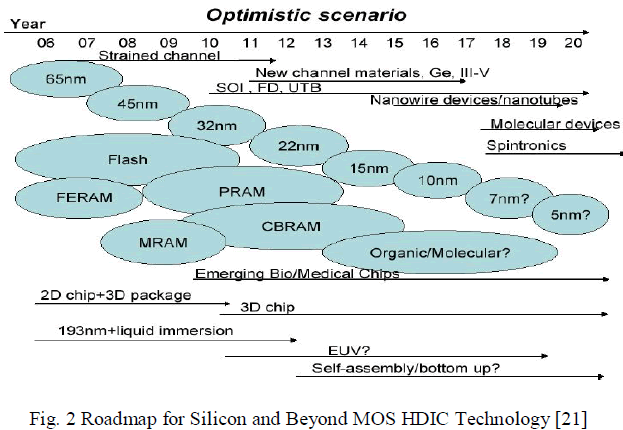
| The development of High Density Integrated Circuits (HDICs) is facing challenges in the further development aiming higher device performances mainly low power consumption and higher frequency operations. Usually, HDICs performances are improved by reducing the MOS transistor’s dimensions. MOSFET dimensions are going down from submicron to nanometre range. However, the drastic dimension reduction will not always comply with device performances if the basic silicon material is not engineered as illustrated in Fig.2 [21]. Advanced MOSFETs that provide a path to scaling CMOS to the end of the time horizon using new transistor structural designs are ultra thin body SOI, the band-engineered transistors, vertical transistors, FINFETs and double gate transistors [22]. UTB scaling provides the extremely thin channel dimensions required to scale CMOS to the 22nm node, improved subthreshold slope and VT controllability. |
 |
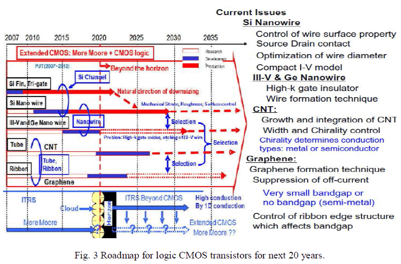
| The long range roadmap for logic CMOS transistors is shown Fig. 3 [22], including the period which ITRS does not cover. The Si-nanowire FETs are the most promising candidates, III–V and Ge-nanowire FETs are the second candidate. However, technical barrier for the fabrication process is much higher compared with the Si nanowire. In future, Carbon Nanowire Transistors and grapheme ribbon FETs could be candidates to replace the Si-nanowire FETs. However, they are still too far at this moment because of no substantial idea for the integration method of so huge number transistor in a chip and bandgap control for high on/off ratio. |
 |
CONCLUSION |
| In this paper we have discussed the present status and future trends of RF CMOS and SOI design and challenges. Si CMOS devices have a cost advantage and are typically used for frequencies up to 2.5 GHz. |
| Most applications above 2.5 GHz will be GaAs-based transistors. High-performance applications above 40 GHz will be dominated by InP-based transistors. It is clear that MOSFETs are progressing quickly and becoming a strong contender in the RF applications traditionally dominated by III–V devices. For high frequency applications the combination of MOSFETs and CMOS-compatible SiGe HBTs (i.e., SiGe BiCMOS) is an excellent option. GaAs-based HBT has been the most widely used HBT in RF design, but SiGe HBT has gained popularity recently due to its superior noise performance and its compatibility with existing Si CMOS technology. However future design consists of multiple gate SOI MOSFETs along with study of effects of temperature on device performance. |
References |
|