ISSN ONLINE(2319-8753)PRINT(2347-6710)
ISSN ONLINE(2319-8753)PRINT(2347-6710)
Ananda S.Paymode.Dnyaneshwar K.Padol. Santosh B.Lukare.
|
| Related article at Pubmed, Scholar Google |
Visit for more related articles at International Journal of Innovative Research in Science, Engineering and Technology
This paper presents a delay measurement technique using signature analysis, and a scan design for the proposed delay measurement technique to detect small-delay defects. The proposed measurement technique measures the delay of the explicitly sensitized paths with the resolution of the on-chip variable clock generator. The proposed scan design realizes complete on-chip delay measurement in short measurement time using the proposed delay measurement technique and extra latches for storing the test vectors. The evaluation with Rohm 0.18- m process shows that the measurement time is 67.8% reduced compared with that of the delay measurement with standard scan design on average. The area overhead is 23.4% larger than that of the delay measurement architecture using standard scan design and the difference of the area overhead between enhanced scan design and the proposed method is 7.4% on average. The data volume is 2.2 times of that of test set for normal testing on average.
Index Terms |
| Delay estimation, design for testability (DFT), integrated circuit measurements, semiconductor device reliability, signature register |
INTRODUCTION |
| With the scaling of semiconductor process technology, performance of modern VLSI chips will improve significantly. However, as the scaling increases, small-delay defects which are caused by resistive-short, resistive-open, or resistive-via become serious problems [1]. If small-delay defects cannot be detected in LSI screening, the chips will behave abnormally under particular operations in certain applications, and their lifetime may become very short due to the vulnerability to the transistor aging. Therefore to keep the reliability after shipping, enhancing the quality of the testing for the small-delay defect detection is an urgent need. The delay measurement of paths inside the circuits is useful for detection and debugging of small-delay defects [2]. However, it is impossible to measure the small circuit path delays using an external tester, even if the resolution is high. Therefore development of the embedded delay measurement technique is required. Some embedded delay measurement techniques have been proposed. The scan-based delay measurement technique with the variable clock generator is one of these on-chip delay measurement techniques [3]. In this technique, the delay of a path is measured by continuous sensitization of the path under measurement with the test clock width reduced gradually by the resolution. The main good point of the scan-based delay measurement technique is its high accuracy. The reason of the high accuracy is that the technique measures just the period between the time when a transition is launched to the measured path and the time when the transition is captured by the flip flop connected to the path, directly. The variation of the measured value just depends on the variation of the clock frequency of the clock generator. Therefore, if the clock generator is compensated the influence of the process variation, the measured value does not depend on the process variation. However, it has a drawback. The measurement time of the technique depends on the time for the scan operation. These days, the gap between the functional clock and scan clock frequency increases. Therefore the measurement time becomes too long to make it practical. Noguchi et al.proposed the self-testing scan-FF. The flip flop reduces the required number of scan operations, which makes the measurement time practical [2]. They also proposed the area reduction technique of the self-testing scan-FF [4]. However, the area overhead of these methods is still expensive compared with the conventional scan designs. This paper presents a scan-based delay measurement technique using signature registers for small-delay defect detection. The proposed method does not require the expected test vector because the test responses are analyzed by the signature registers. The overall area cost is of the order of conventional scan designs for design for test (DFT). The measurement time of the proposed technique is smaller than conventional scan-based delay measurement. The extra signature registers can be reused for testing, diagnosis, and silicon debugging. These days, various methods for small-delay defect detection have been proposed. The path delay fault testing with a normal clock width is the most popular and is widely used. In this method, we choose the longer paths to detect the smaller cumulative delay due to the small delay distributed on the paths. The larger the cumulative delays, the higher the probability of the detection of the distributed small delay. However, the coverage of the small delay defect detection largely depends on the normal clock width, which is a problem of this method. On the other hand, to solve the problem, methods with delay fault testing using a variable clock generator have been proposed. The delay fault testing with a smaller test clock reduces the slack of the paths. Therefore the smaller delay defects which cannot be captured with the normal clock width can be captured with the appropriate smaller test clock width. Liou et al. proposed a small-delay defect detection method consisting of two test phases using both a tighter test clock and a normal clock. In this method, the transition delay fault testing with a tighter test clock width which is calculated based on the characterized delay distribution is applied in the first phase. After that, path or transition delay fault testing is applied with a normal clock width in the second phase. The quality of the method is higher than the conventional one phase test with normal clock width. Yan et al. proposed a delay testing scheme that identifies small-delay defects in the slack interval by comparing switching delays of a neighboring die on a wafer. In this method, a fault site is sensitized multiple times continuously with reducing the test clock width by the slack interval. The abnormal switching delays are detected by comparison with the test results in the neighboring die. Another work detects small-delay defects by analyzing the failing frequency, which is the minimum frequency that the delay fault testing fails when the path is sensitized multiple times continuously with increasing the test clock frequency. Generally, the variable clock testing requires a variable on-chip clock generator. |
| Various variable on-chip clock generators have been proposed. In variable clock testing, the test clock frequency should be optimized to each test vector. To improve the test quality, various optimization methods of the test clock and test set have been proposed these days, small-delay defect detection methods using on-chip delay measurement techniques have been proposed. The direct measurement of the real delay of each path of each chip screens outlier chips robustly even in the presence of process variation or the gap between real and simulation environment. It realizes higher fault coverage of small-delay defects than the simulation- based ones. In addition, it can be used not only for the detection of small delay defects, but also for the debugging Because modern chips are too huge and complex, LSI CAD tools cannot optimize the design enough. Hence, the manufactured first silicon chip usually does not meet the specification in spite of the tighter release to production (RTP) schedule. Therefore silicon debugging and design for debugging (DFD) become much more important in modern chips various silicon debugging technologies and DFD methods have been proposed On-chip delay measurement provides accurate information of the delay of inside paths for the debugging of small-delay defects. Most of the conventional works of on-chip delay m measurement are classified to either a proposal of an embedded delay On-chip variable clock generator measurement circuit or that of scan architecture for scan-based onchip delay measurement with a variable clock generator |
II. DESIGN CONCEPT |
| With the scaling of semiconductor process technology, performance of modern VLSI chips will improve significantly. However, as the scaling increases, small-delay defects which are caused by resistive-short, resistive-open, or resistive-via become serious problems. If small-delay defects cannot be detected in LSI screening, the chips will behave abnormally under particular operations in certain applications, and their lifetime may become very short due to the vulnerability to the transistor aging. Therefore to keep the reliability after shipping, enhancing the quality of the testing for the small-delay defect detection is an urgent need. The delay measurement of paths inside the circuits is useful for detection and debugging of small-delay defects. However, it is impossible to measure the small circuit path delays using an external tester, even if the resolution is high. Therefore development of the embedded delay measurement technique is required. Some embedded delay measurement techniques have been proposed. |
| The scan-based delay measurement technique with the variable clock generator is one of these on-chip delay measurement techniques. In this technique, the delay of a path is measured by continuous sensitization of the path under measurement with the test clock width reduced gradually by the resolution. The main good point of the scan-based delay measurement technique is its high accuracy. The reason of the high accuracy is that the technique measures just the period between the time when a transition is launched to the measured path and the time when the transition is captured by the flip flop connected to the path, directly. The variation of the measured value just depends on the variation of the clock frequency of the clock generator. Therefore, if the clock generator is compensated the influence of the process variation, the measured value does not depend on the process variation. However, it has a drawback. The measurement time of the technique depends on the time for the scan operation. These days, the gap between the functional clock and scan clock frequency increases. |
| Therefore the measurement time becomes too long to make it practical. Noguchi et al. proposed the self-testing scan-FF. The flip flop reduces the required number of scan operations, which makes the measurement time practical. They also proposed the area reduction technique of the self-testing scan-FF. However, the area overhead of these methods is still expensive compared with the conventional scan designs. This paper presents a scan-based delay measurement technique using signature registers for small-delay defect detection. The proposed method does not require the expected test vector because the test responses are analyzed by the signature registers. The overall area cost is of the order of conventional scan designs for design for test (DFT). The measurement time of the proposed technique is smaller than conventional scan-based delay measurement. |
Variable Clock Generators |
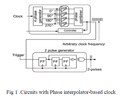
| In the proposed method, the clock width should be reduced continuously by a constant interval as explained later. It is difficult for an external tester to control this clock operation. Therefore an on-chip variable clock generator is indispensable for the proposed method. In this paper, we use the on-chip variable clock generator proposed by Noguchi et al .Fig. 1 illustrates the circuit. The circuit consists of the phase interpolator-based clock generator and the 2-pulse generator. The phase-interpolator-based clock generator generates an arbitrary clock width. The 2-pulse generator generates 2-pulse test clocks with arbitrary timing in response to a trigger signal. |
 |
Small-Delay Defect Detection with Delay Measurement of Chip |
| The proposed method uses the Noguchi’s small-delay defect detection technique. In this technique, the test clock width for delay fault testing of each path is determined with the normal path-delay distribution of each path. This strategy has already been applied to various small-delay detection techniques. But its originality is to obtain the path-delay distribution with the delay measurement of the paths of the fabricated chips. Fig. 2. Shows the path delay distribution of a path obtained by the delay measurement of the fabricated sample chips. The horizontal axis is measured delay. The vertical axis is the number of chips. The chips which have delay inside the range Variation are normal chips. The chips which have delay outside the range Variation, namely, are abnormal chips. The delay is the outside of the clock cycle in normal operation. Therefore it will be detected by conventional delay fault testing with the clock cycle in normal clock operation which is Conventional criteria. The delay and are within the clock cycle in normal operation. In Noguchi’s technique, the test clock cycle is set to the upper limit of the distribution of normal chips, which is a new criterion. Then all the outlier chips are detected by the delay fault testing. In small technology, the path-delay distribution calculated by simulation is different from that of the fabricated chips. Therefore the quality of its strategy is higher than that of simulation based ones. Because the Noguchi’s technique requires the measurement of the explicit paths, the paths should be single-path sensitizable. The aim of the technique is to screen the chips which have abnormal delay in gates or wires. Therefore the test set for the measurement should detect all the transition faults which are sensitized through single-path sensitizable paths. The proposed method is a new delay measurement technique for the small-delay defect detection technique. |
 |
2.4 Delay Measurement techniques using signature analysis |
| This section explains the proposed measurement method. Section III-A presents the concepts of the proposed method. Section IIIB explains the implementation of the proposed method. Section III-C describes the measurement sequence. The data volume and area overhead should be realistic compared with the conventional scan designs for DFT. Section III-D explains the reduction method of the tester channel. Section III-E describes the scheme for the decision of the number of the required extra latches to keep the cost realistic. To apply the proposed method and realize short measurement time, some constraints should be put on ATPG. Section III-F explains the ATPG constraints. Section III-G describes the measurement time and data volume. Finally, Section III-H describes the test response tracing mode for finding lowest failing frequency or diagnosis with transition fault test vectors. This section explains the concept of the proposed delay measurement. The target paths of the proposed method are single path sensitizable. Basically, the proposed method is scan-based delay measurement. The difference from the basic one is the usage of the signature registers and the additional latches for the acceleration of the delay measurement. |
 |
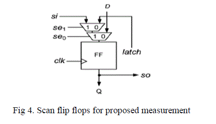
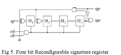
| This example has three flip flops. Each flip flop has the input line (bottom), the output line (upper), and the clock line. Each flip flop is connected to an extra latch. At first, we assume that each flip flop has its own extra latch. The value of each flip flop is stored in the correspondent latch, and the value of each latch can be loaded to the correspondent flip flops in arbitrary tim ing. In the proposed measurement, the test vector is stored in these latches after scan-in operation. Once the test vector is stored in the latches, the test vector can be loaded from these latches in a clock without scan-in operation. It reduces the time for multiple sensitization of a path drastically. The horizontal line through these flip flops represents the scan path. The symbols and represent the scan input and output, respectively. The rectangle SIG represents the signature register using the linear feedback shift register as its basic component. The input of SIG is connected to the output of the last flip flop. More detail structures of the flip fops and the signature register are shown in Figs. 4 and 5 respectively. |
 |
 |
| Here, we measure the delay of. In this example, we assume that the clock width of normal operation is 10 ns, and the resolution of the delay measurement is 2 ns. First, SIG is initialized with reset operation. Second, the target path is tested continuously 5 times with the test clock reduced gradually by the resolution. The multiple clock width testing is realized by the variable clock generator explained in Section II-B. The test clock of the 1st testing (#1) is 10 ns. After the test, the test response is sent to SIG through the scan path with two clock shift out operation. The test clock of the second testing (#2) is 8 ns. Similarly, the test clock width of the third, fourth, and fifth testing’s (#3, #4, #5) are the difference between 2 ns and the previous test clock width. Each test response is sent to SIG with two clocks. After the above 5 times of delay fault testing’s, the signature value of SIG is retrieved. To estimate the delay, the retrieved signature value is compared with the expected signature values of the signature table. Fig. 2.3(b) shows the signature table in this example. The table has four columns. The first column is the cases of the measurement. The second column is the sequences of the test responses of #1–#5. The third column is the path delay value. The fourth column is the signature values of each case. Here, and are the signature values for rising and falling transition testing’s, respectively. The delay of each path is decided as more than 10, 8–10, 6–8, 4–6, 2–4, or 0–2ns, with 2ns resolution. The sequences of the test responses of the 5 times measurement are shown in Fig. 2.3(b). The symbols , , , , , indicate the cases with path delays, more than 10, 8–10, 6–8, 4–6, 2–4, 0–2 ns, respectively. The symbols and represent the pass and fail of a testing, respectively. In case of rising transition testing, and, and in case of falling transition testing, and. The retrieved signature value is compared with the expected signature values on the table, and decides the delay value. When the number of flip flops is, clock width is, the measurement resolution is, and the continuous testing time is, the delay measurement sequence of a target path is as follows. Here, we assume that the test vector is already stored in the latches. The end point of the measured path is |
| Step 1: Initializing SIG. |
| Step 2: Test vector is loaded from the latches. |
| Step 3: Test clock width is set to normal clock width. |
| Step 4: Test clock is applied. |
| Step 5: The test response is sent to SIG which is connected to the output of with clocks. |
| Step 6: If testing time is equal to , go to Step 7 after The signature value of SIG is retrieved, otherwise go Back to Step 2 after the test clock width is updated to . |
| Step 7: The delay value is estimated by comparing the retrieved signature value and the signature table. |
III. INTRODUCTION OF FPGA |
| As described in Architectural Overview, the Spartan™-3E FPGA architecture consists of five fundamental functional elements: |
 |
| Powering Spartan-3E FPGAs Input/ Output Blocks (IOBs) The Input/ Output Block (IOB) provide a programmable, unidirectional or bidirectional interface between a package pin and the FPGA’s internal logic. The IOB is similar to that of the Spartan-3 family with the following differences: Input-only blocks are added Programmable input delays are added to all blocks DDR flip-flops can be shared between adjacent IOBs The unidirectional input-only block has a subset of the full IOB capabilities. Thus there are no connections or logic for an output path. The following paragraphs assume that any reference to output functionality does not apply to the input-only blocks. The number of input-only blocks varies with device size, but is never more than 25% of the total IOB count.Figure 6. Is a simplified diagram of the IOB’s internal structure.There are three main signal paths within the IOB: the output path, input path, and 3-state path. Each path has its own pair of storage elements that can act as either registers or latches. For more information, see Storage Element Functions. The three main signal paths are as follows: The input path carries data from the pad, which is bonded to a package pin, through an optional programmable delay element directly to the I line. After the delay element, there are alternate routes through a pair of storage elements to the IQ1 and IQ2 lines. The IOB outputs I, IQ1, and IQ2 lead to the FPGA’s internal logic. The delay element can be set to ensure a hold time of zero (see Input Delay Functions).The output path, starting with the O1 and O2 lines, carries data from the FPGA’s internal logic through a multiplexer and then a three-state driver to the IOB pad. In addition to this direct path, the multiplexer provides the option to insert a pair of storage elements. The 3-state path determines when the output driver is high impedance. The T1 and T2 lines carry data from n the FPGA’s internal logic through a multiplexer to the output driver. In addition to this direct path, the multiplexer provides the option to insert a pair of storage elements. All signal paths entering the IOB, including those associated with the storage elements, have an inverter option. Any inverter placed on these paths is automatically absorbed into the IOB. |
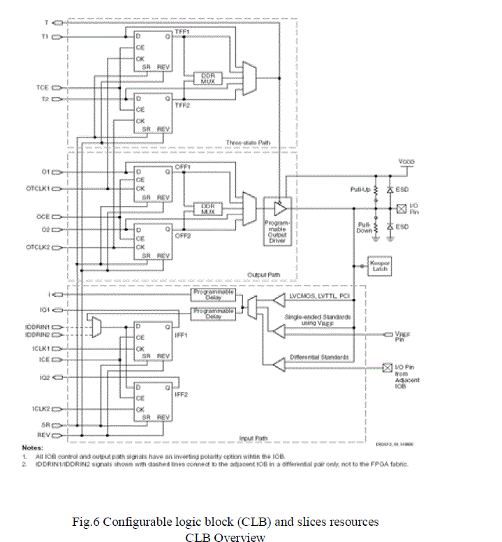 |
| The Configurable Logic Blocks (CLBs) constitute the main logic resource for implementing synchronous as well as combinatorial circuits. Each CLB contains four slices, and each slice contains two Look-Up Tables (LUTs) to implement logic and two dedicated storage elements that can be used as flip-flops or latches. The LUTs can be used as a 16x1 memory (RAM16) or as a 16-bit shift register (SRL16), and additional multiplexers and carry logic simplify wide logic and arithmetic functions. Most general-purpose logic in a design is automatically mapped to the slice resources in the CLBs. Each CLB is identical, and the Spartan- 3E family CLB structure is identical to that for the Spartan-3 family. CLB ArrayThe CLBs are arranged in a regular array of rows and columns as shown in Figure 6 Each density varies by the number of rows and columns of CLBs |
III SIMULATION RESULT |
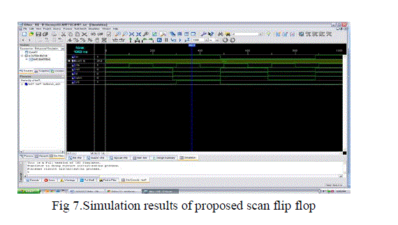 |
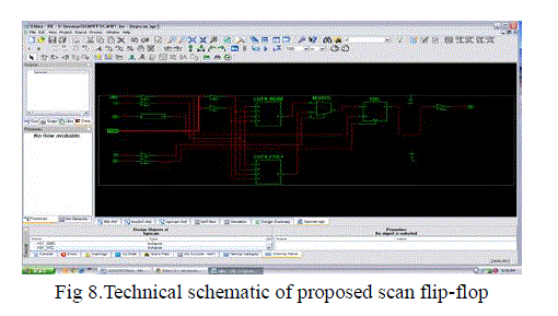 |
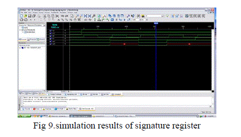 |
IV. CONCLUSION |
| The proposals of this paper are as follows. The proposal of the delay measurement method using signature analysis and variable clock generator. The proposal of a scan design for the delay measurement of internal paths of SoC. The first proposal can be applied not only SoC but also field programmable gate array (FPGA). Because the process of FPGA is getting extraordinary smaller these days, the small delay defect becomes serious problem in FPGA, too. In this meaning, the application of the proposed method to FPGA is also useful. A future work is the low cost application of the proposed measurement to FPGA. When we measure short paths the measurement error can increase for the IR drop induced by higher test clock frequency. It can reduce the test quality. Another future work is the reduction and the avoidance of the measurement error caused by the IR drop. |
V. ACKNOWLEDGMENT |
| Finally, we are thankful to all for the encouragement and support .We are also thankful to our respected principal, HOD and my dear collegue for their effort to make this paper as good as it is. We are also thankful our family member and friend for such excellen.. |
References |
|