ISSN ONLINE(2319-8753)PRINT(2347-6710)
ISSN ONLINE(2319-8753)PRINT(2347-6710)
Sumita Mishra 1, Naresh k. Chaudhary 2, Kalyan Singh 2
|
| Related article at Pubmed, Scholar Google |
Visit for more related articles at International Journal of Innovative Research in Science, Engineering and Technology
The volume of data being transferred between on-chip functional blocks is rising fast due to the need for higher resolution, greater CPU power. Moreover distributed multi-processor architectures require organised high-speed communication between processors. Metallic interconnect is highly inefficient in this role due to unachievable tradeoffs between design parameters and its performance deteriorates rapidly at frequency above 10 GHz due to skin effect and dielectric limitations. Optical interconnects are seen as a viable alternative to electrical interconnects The objective of the work is to model and then simulate the VCSEL based optical interconnect link. The model is based on multimode rate equations and it also accounts for the thermal dependence of a VCSEL’s behaviour. The power output of the simulated link is then optimized with respect to parameters namely optical power and bias current. The methodology presented here is suitable for investigation of both analog and digital modulation schemes but it primarily deals with digital modulation.
Keywords |
| Optical interconnections, Bit error rate, VCSEL’s, Optical receiver |
INTRODUCTION |
| The microprocessor industry has developed at an incredible pace, particularly in the past decades. Transistor scaling has been the crux of the rapid growth in processing power over the past forty years [1]. Increased processing power has resulted in tremendous increase in microprocessor’s clock speed and cache size moreover multiple cores and hyper threading has increased the complexity of these systems. These multicore ultrafast processors require high speed data transmission that allows individual processors fast access to memory, its cores and other I/O devices. Interconnects are the communication system that provides channels to transmit data. As speed and complexity of these systems increase the interconnect density and throughput management becomes a critical factor towards the realization of high performance data processing systems. Currently copper interconnects are used for data transmission over chip-to-chip and chip-to-module interfaces, in chip-to-chip over backplane, and in chip-to-chip over copper cable assemblies. Electrical interconnects performance degrades at frequencies above 1 GHz due to ringing, increased signal latency, crosstalk and frequency dependent attenuation [1]. These limitations of electrical interconnects will limit the maximum frequency of operation for future systems; Optical interconnect is seen as a potential solution since it can directly address these problems at the system level and meet the performance requirements of current and future generation of data processors, optical interconnects have negligible frequency dependent loss, low cross talk and high band width. Advantages offered by optical interconnects provide strong motivation to further develop methodologies for analysing optical interconnect links. Analysis of high speed optical interconnects link is MATLAB and Simulink may be a powerful tool since it offers multi-domain simulation environment and model-based design which can accurately model the behaviour of optical sub systems making it a good platform for optimization of optical interconnect link. |
II. BACKGROUND |
| Vertical Cavity Surface Emitting Laser (VCSEL) is currently the most attractive optical source for the short-distance optical interconnects. A Vertical Cavity Surface-Emitting Laser (VCSEL) is a semiconductor laser diode that emits light perpendicular to the upper surface of the semiconductor wafer of which the laser is composed. Monolithic arrays of high density VCSELs manufactured for several different wavelengths [9] have been developed by various manufacturers which are competitively priced. choice for an ultra-dense chip-to-chip level interconnects, operating at data rates in the range of Tb/s . During the recent years there has been a significant development effort towards VCSELs operating at a wavelength range of 1200…1600 nm using the InP-based process technology. VCSELs operating at a wavelength near 1550 nm have the disadvantage of growth difficulties and low thermal conductivity of the necessary DBRs. [11] VCSELs offer many of the desirable characteristics of an optoelectronic transmitter for optical interconnects. 2D arrays of high speed VCSEL with good contrast at a low voltage drive can be fabricated. Recent advances in VCSEL technology [12] along with research into new materials such as InGaNAs(Sb) has shown promise for higher data rates with low power consumption in the near future. Thus VCSEL based transmitters are likely to be used in optical interconnect applications.There have been several attempts at optimizing optical interconnect links using software tools such as Microsim P-Spice. [3-6] P-Spice is designed for EDA and is not optimized for optical networks hence at very high frequencies precision of simulated circuit reduces. We have used MATLAB and Simulink tool for modelling and simulation of high speed VCSEL based optical interconnect transmitter. |
III MODELING AND SIMULATION METHODOLOGY |
| In this section we describe the methodology used for modelling and simulation of optical interconnect transmitter. The simulated VCSEL diode is an InGaAs–Al-GaAs–GaAs quantum-well separate confinement heterostructure. For simulation of the dynamic response of VCSEL a rate equation model has been used [2]. |
 |
| where S is the photon number, N is carrier number, P0 is optical output power, ηi is the injection efficiency, τn is the carrier recombination lifetime, G0 is the gain coefficient, N0 is the carrier transparency number, τp is the photon lifetime, β is the spontaneous emission coupling coefficient, and ε is the gain-compression factor. k is a scaling factor accounting for the output coupling efficiency of the VCSEL. |
IV. MODEL DESCRIPTION AND RESULTS |
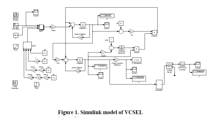
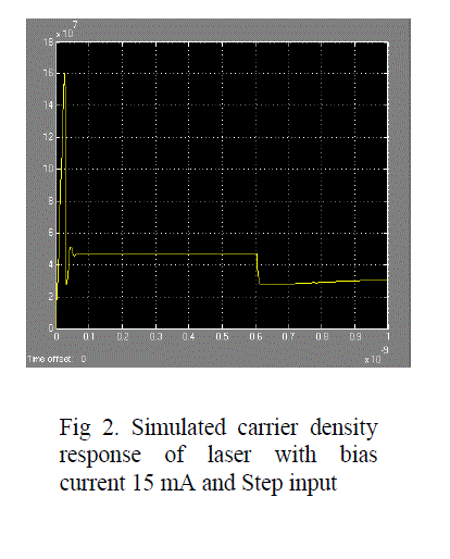
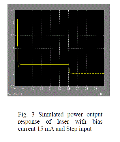
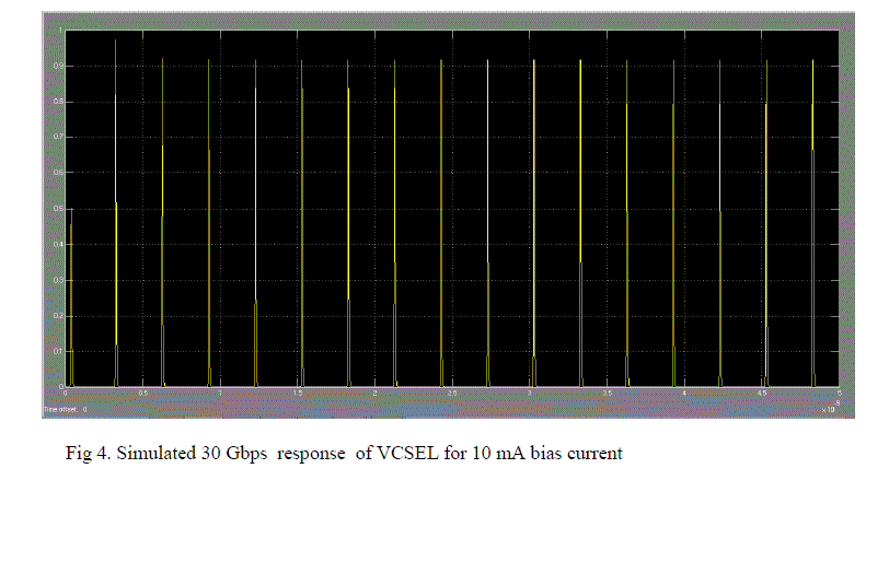
| The rate equations described in previous section were implemented in simulink as shown in fig -1. Transient analysis of simulated laser was performed and it can be seen from fig 2 and 3 that the simulated laser power output is stable and non oscillatory in nature. Response of laser to the step input and 15 mA bias current is shown in fig 2. Simulated optical power output of laser with ramp input and bias current=15mA is shown in fig 3. It can be seen from the figure 3 that there is certain delay in obtaining the power output after application of step input last figure thus the simulated optical output power shows the expected laser turn-on delay. After the transient response laser was subjected to a pulse train of 5% duty cycle and laser output was obtained for different frequencies . All the simulations were run over a time period that was several orders of magnitude longer than the fixed step size chosen so that turn-on transient effects that happen near threshold can be avoided. All simulations used a standard 4th-order Runge-Kutta algorithm with a fixed step size. Figure 4 shows laser response to 30 Gbps data rate at 10 mA bias current.It can be seen from figure 4 that simulated laser output is as expected. |
 |
 |
 |
 |
V. CONCLUSION |
| CMOS technology scaling and efficient time-division multiplexing architectures have led electrical link data rates to the point where the channel bandwidth is the current performance bottleneck. Optical inter-chip links offer a promising solution to this I/O bandwidth problem due to the optical channel’s negligible frequency dependent loss. Thus optical interconnects have the potential to fully leverage CMOS technology advances with efficient interconnect architectures and low-power circuit techniques. The work addressed optical source issues which include accurate simulation and reliable driving of The behaviour of VCSEL Laser is modelled with a set of three differential equations which describe the mechanism by which an electrical current causes stimulated photon emission The modulator was simulated on MATLAB Simulink tool and various results described in section III were obtained. We have not included the effect of carrier charge density in multiple quantum well. The model can be further improved by including photon noise terms. |
References |
|