ISSN ONLINE(2319-8753)PRINT(2347-6710)
ISSN ONLINE(2319-8753)PRINT(2347-6710)
Yogesh Dagur1, Dr. Mukesh Kumar Gupta2
|
| Related article at Pubmed, Scholar Google |
Visit for more related articles at International Journal of Innovative Research in Science, Engineering and Technology
In single phase AC-DC converter employing power factor correction here we intend to produce a programmable power supply those whose output voltage can be varied as per user requirement. The paper propose the power factor correction technique, single phase active power factor correction, circuit configurations and results for the single phase AC-DC converter.
Keywords |
| Power factor, AC-DC converter, Buck converter, power factor correction (PFC), Boost converter |
INTRODUCTION |
| AC-DC converter with high frequency transformer is most widely used in switched mode power supply (SMPS), battery charging, uninterrupted power supply (UPS), electronic ballast, induction heater. SMPS works like a DC chopper by operating the on/off switch rapidly, AC ripple frequency rises which can be easily filtered by L and C filter circuits which are small in size and less in weight. It may therefore be inferred that is the requirement of small physical size and weight that has led to the wide spread use of SMPSs. If the switching devices are power transistor, the chopping frequency limited to 40 kHz. For power MOSFETs the chopping frequency is of the order of 200 kHz as a result size of the filter circuit and transformer decreases leading to considerable savings. as such high frequency, ferrite core is used in transformers. The overall size of SMPS it depend on operating frequency. Use of power transistor is limited to approximately 40-50 kHz. Above this operating frequency, power MOSFET is used up to above 200 kHz. The paper proposes to make single phase AC-DC converter with maintaining power factor close to unity. By implementing two stages we produce programmable power supply to overcome the problem of power quality in terms of harmonic current at AC mains voltage distortion, reduced power factor, high peak factor and require a large size of dc capacitor filter at first stage. This AC-DC converter mainly used to improve the power quality and to reduce the number of components and to improve the efficiency. A buck–boost-type unity power factor rectifier is pro- posed in this paper. The main advantage of the proposed rectifier over the conventional buck–boost type is that it can perform input power factor correction (PFC) over a wider voltage conversion range. With a single switch, a fast well-regulated output voltage is achieved with a zero-current switch at turn-on. Moreover, the switch voltage stress is independent of converter load variation. Finally the buck-boost converter are classified into fly back, cuk, SEPIC, and ZETA converter. This type of converter are controlled by the different control method as DSP, Microcontroller, and improved high efficiency buck, boost, buck-boost topologies with high frequency transformer isolation. Depending upon the voltage level require at the consumer side, the ac main voltage is connected into dc power to feed variety of loads through the single phase ac-dc converter, classified into buck, boost, buck-boost converter to improve the power quality at ac mains and dc loads. These converters are implemented using high frequency transformer isolation with single or multiple converters such as buck, boost, and buck-boost topologies. One of the major reasons to develop the ac-dc converter is the availability of high frequency with switching devices like MOSFET which has the high switching capability with negligible losses. |
II. POWER FACTOR CORRECTION TECHNIQUES |
| In previous years, single-phase switch-mode AC/DC power converters have been increasingly used in the commercial, industrial, aerospace, residential, and military environment due to advantages of high smaller size, efficiency and weight. However, the proliferation of the power converters draw pulsating input current from the utility line, this not only reduce the input power factor of the converters but also injects a substantive amount of harmonic current into the utility line [1]. To improve the power quality, various PFC schemes have been proposed. There are harmonic norms such as IEC 1000-3-2 introduced for improving power quality. By the introduction of harmonic norms now power supply manufacturers have to follow these norms strictly for the remedy of signal interference problem [2]. The various methods of power factor correction can be classified as: (1) Passive power factor correction techniques (2) Active power factor correction techniques |
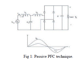
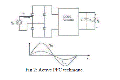
| In passive power factor correction techniques, an LC filter is inserted between the AC mains line and the input port of the diode rectifier of AC/DC converter as shown in Figure 1. This technique is rugged and simple but it has heavy weight and bulky size and there will be the power factor cannot be very high [1]. Therefore it is now not applicable for the current trends of harmonic norms. Fundamentally it is applicable for power rating of lower than 25W. For higher power rating it will be bulky. In active power factor correction techniques approach, switched mode power supply (SMPS) technique is used to shape the input current in phase with the input voltage. Thus, the power factor can reach up to unity. Figure 2 shows the circuit diagram of basic active power correction technique [2]. By the introduction of regulation norms IEC 1000-3-2 active power factor correction technique is used now a day. There are different topologies for implementing active power factor correction techniques. Fundamentally in this technique power factor correcting cell is used for tracking the input current in phase of input voltage such that input power factor come up to unity. Comparing with the active PFC techniques, passive PFC techniques have many advantages such as reduced harmonics, high power factor, smaller size and light-weight. However, the relatively and complexity higher cost are the main drawbacks of this approach. |
 |
 |
| The active PFC techniques can be classified as: (1) PWM power factor correction techniques (2) Resonant power factor correction techniques (3) Soft switching power factor correction techniques |
| PWM power factor correction approach, the power switching device operates at pulse-width-modulation (PWM) mode. Fundamentally in this technique switching frequency of active power switch is constant, but turn-off and turn-on mode is variable. The advantage is ease of analysis and control, simple configuration, current stress and lowest voltage. Therefore it is extensively used in PFC circuits. For the minimization of converter size PWM technique generates significant switching loss. Different topologies of PWM techniques are as follows: (1) Buck type |
| (2) Flyback type (3) Boost type (4) CukâÃâ¬ÃŸ type |
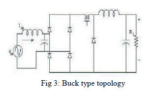
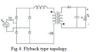
| Figure 3 shows the buck type topology. Its advantage of buck type topology is that the converter can supply a low output voltage with respect to input voltage. The disadvantages are, significant current distortion, EMI is higher because discontinuous input current so filter design is costly. It is a basic DC-DC converter and it is not used for power factor correction [1]. Figure 4 shows the flyback type topology. The advantages are, output voltage can be lower or higher than input voltage and i/p and o/p can be isolated. The disadvantages are higher switching device voltage and current rating, input current is discontinuous so requirement of careful design of input filter, difficult to program the input current with current mode control [1]. |
 |
 |
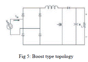
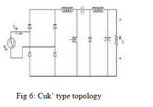
| The boost type topology is shown in Figure 5. The Advantages of this topology are current mode control is easy and less EMI so it reduced input filtering requirements. The main disadvantages are more, no isolation, conduction loss and output voltage is always higher than input voltage [1]. The CukâÃâ¬ÃŸ type is shown in Figure 6. Its advantages are, input current remains continuous even if the converter operates in discontinuous conduction mode, and also the output voltage can be lower or higher than the instantaneous input voltage. Disadvantages are the increased voltage and current stress on power devices, capacitor and requirement of extra inductor and isolation is not provided [3]. |
 |
 |
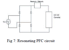
| In the resonant converter, the voltage across a switch or the current through a switch is shaped by the resonance of capacitor and inductor to become „0âÃâ¬ÃŸ at the time of turned on or off. Thus the switching loss is greatly reduced. The high power factor is achieved by the natural gain-boosting characteristic of the resonant converter. The major disadvantages are higher voltage and current stress on the power switch with respect to PWM mode and variable switching frequency employed. Figure 7 shows a PFC circuit in which a resonant converter is inserted between the DCDC converter and the input diode rectifier. This resonant converter can be series resonant converter or a charge pump resonant network [3]. The advantage is that the current stress and voltage stress on resonant components as well as power switches are lower than the previous resonant converter [1]. |
 |
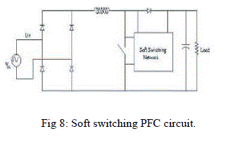 |
| The soft-switching PFC technique combines the advantages of PWM mode and resonant mode techniques with an additional resonant network consisting of a resonant capacitor, a resonant inductor and an auxiliary switch. The AC/DC converter operates in PWM mode during most portion of a switching cycle but operates in resonant mode during the switch turn-off and turn-on intervals. As a result, the PFC circuit power switch turns on and off at zero current or zero voltage conditions and works at constant switching frequency. Thus efficiency and power factor both improved by this technique. Figure 8 shows boost PFC circuit with a soft switching network [1]. |
III. SINGLE PHASE ACTIVE POWER FACTOR CORRECTION |
| Conventional off-line power converters with diode capacitor rectifier front-end have distorted input current waveform with high harmonic content. They cannot meet neither the European line-current harmonic regulations defined in the IEC1000-3-2 document or the corresponding Japanese input-harmonic current specifications. To meet the requirements of above norms it is customary to add a power factor corrector ahead of the isolated dc/dc converter section of the switching power supply. Again another dc/dc converter is needed for output voltage regulation. Thus there are two converter is needed for single-phase active power factor correction for the requirement of high input power factor and tight output regulation. There are two approaches for single-phase active power factor correction: (1) Two-stage approach (2) Single-stage approach |
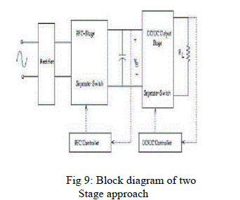
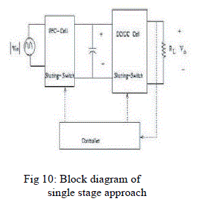
| Two-stage approach is commonly used approach in high power applications [4]. The block diagram of two stages PFC converter is shown in Figure 9. In this approach, there are two independent power stages. The front-end PFC stage is usually a boost or buck-boost (or flyback) converter. The dc/dc output stage is the isolated output stage that is implemented with at least one switch, which is controlled by an independent PWM controller to tightly regulate the output voltage. The two-stage approach is a cost-effective approach in high power applications; its cost-effectiveness is diminished in low-power applications due to the additional PFC power stage and control circuits. A single-stage scheme combines the PFC circuit and dc/dc power conversion circuit into one stage. A number of single-stage circuits have been reported in recent years. Figure 10 shows the block diagram of single-stage approach. Compared to the two-stage approach, the single approach uses only one switch and controller to shape the input current and to regulate the output voltage. Although for a single-stage PFC converter attenuation of input-current harmonics is not as good as for the two-stage approach. But it meets the requirements of IEC1000-3-2 norms. Again it is cost effective and compact with respect to two stage approach [4]. |
 |
 |
| There are four possible combinations to obtain different single stage single switch PFC converters [5]: (1)Discontinuous Conduction Mode PFC + Continuous Conduction Mode DC/DC (2)Discontinuous Conduction Mode PFC + Discontinuous Conduction Mode DC/DC (3) Continuous Conduction Mode PFC + Continuous Conduction Mode DC/DC (4) Continuous Conduction Mode PFC + Discontinuous Conduction Mode DC/DC |
IV. POWER FACTOR WITH LOADS |
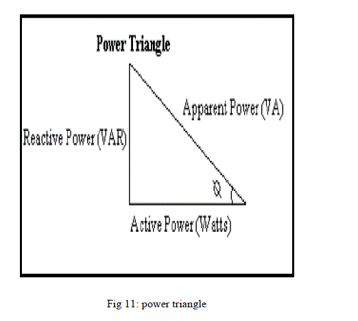
| Power factor is defined as the cosine of the angle between voltage and current in an AC circuit. If the circuit is inductive, the current lags behind the voltage and power factor is referred to as lagging. However, in a capacitive circuit, current leads the voltage and the power factor is said to be leading |
 |
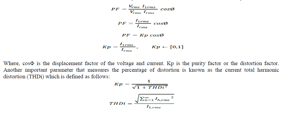
| 1) Linear Systems: In a linear system, the load draws purely sinusoidal current and voltage; hence the power factor is determined only by the phase difference between voltage and current. 2) Nonlinear Systems: In nonlinear systems like power electronic systems, due to the non-linear behaviour of the active switching of power devices, the phase angle representation alone is not valid. A nonlinear load draws typical distorted line current from the line. For sinusoidal voltage and non- sinusoidal current the PF can be expressed as: |
 |
V. RECTIFIERS |
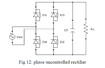 |
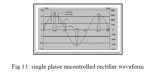
| Generally uncontrolled rectifiers are connected directly to a DC smoothing capacitor. Fig. 13 shows its input voltage and current waveforms. |
 |
| 2) Controlled Rectifier: Controlled rectifiers are used in variable speed DC drives DC power plants, induction heating and welding furnace control, etc. Fig. 14 shows the circuit diagram of the single-phase fully controlled rectifier. |
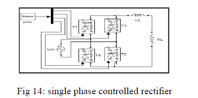 |
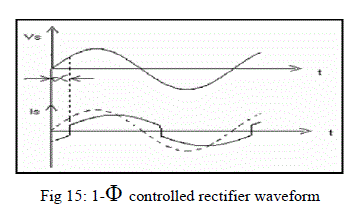
| The controlled rectifier is normally connected to a smoothing inductor on the DC side. Thus the output current of the controlled rectifier could be considered as constant. Fig 15 shows the input voltage and current waveforms. |
 |
VI. NEED FOR IMPROVEMENT OF POWER FACTOR |
| `Conventional AC rectification is thus a very inefficient process, resulting in waveform distortion of the current drawn from the mains. This produces a large spectrum of harmonic signals that may interfere with other equipment. At higher power levels (200 to 500 watts and higher) severe interference with other electronic equipment may become apparent due to these harmonics sent into the power utility line. Another problem is that the power utility line cabling, the installation and the distribution transformer, must all be designed to withstand these peak current values resulting in higher electricity costs for any electricity utility company. Conventional AC rectification has the following main disadvantages: |
| 1) It creates harmonics and electromagnetic interference (EMI). 2) It has poor power factor. 3) It produces high losses. 4) It requires over-dimensioning of parts. 5) It reduces maximum power capability from the line. |
| a. Active PFC Methods: An active approach is the most effective way to correct power factor of electronic supplies. Here, we place different Active PFC converters between the bridge rectifier and the load. The converter tries to maintain a constant DC output bus voltage and draws a current that is in phase with and at the same frequency as the line voltage. Advantages: |
| 1) Active wave shaping of the input current 2) Filtering of the high frequency switching 3) Feedback sensing of the source current for waveform control 4) Feedback control to regulate output voltage |
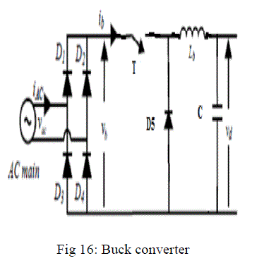
| i). Buck Converter: A buck converter based PFC circuit that steps down the input voltage are shown in Fig. 16 However since the converter can operate only when the instantaneous input voltage Vin(t) is higher than the output voltage Vo, there is no current flow from the AC input during the period t1 and t2. This gives the line current envelope a distortion near the input voltage zero crossing. Moreover, even if the inductor current is continuous, the input switching current of the converter is discontinuous as the high frequency switch. |
 |
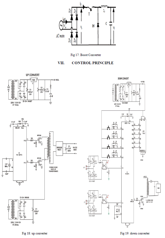
| ii). Boost Converter: The key principle that drives the boost converter is the tendency of an inductor to resist changes in current. When being charged it acts as a load and absorbs energy (somewhat like a resistor). When being discharged it acts as energy source (somewhat like a battery). The fig 17 shows Boost Converter Circuit. The voltage it produces during the discharge phase is related to the rate of change of current, and not to the original charging voltage, thus allowing different input and output voltages. |
 |
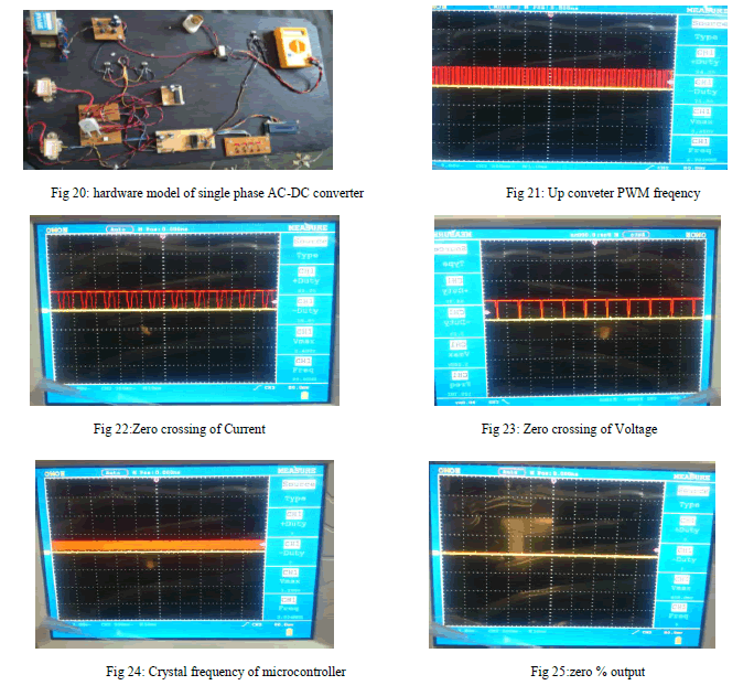
| Development of a single phase AC to DC power supply achieving high power factor and thus high efficiency also. We intend to produce a programmable power supply those whose output voltage can be varied as per user requirement. All this can be achieved using a simple low cost 8-bit microcontroller. The author also intends to provide an LCD display. We will show the various parameter PWM ratios. As per the proposed work the above said power supply will be developed and a variable voltage from 0-50 volt DC on a 220 volt AC 15 watt load (15 watt bulb) will be achieved by employment of high frequency isolation transformer operating in buck-boost mode driven by microcontroller generated PWM signal. |
VIII. RESULT |
| Here in the output result we have waveforms of up converter PWM frequency, when zero crossing of current and zero crossing of voltage. Then we have waveform of crystal frequency of microcontroller, output at 0%, 5%, 95% and on 100%. |
 |
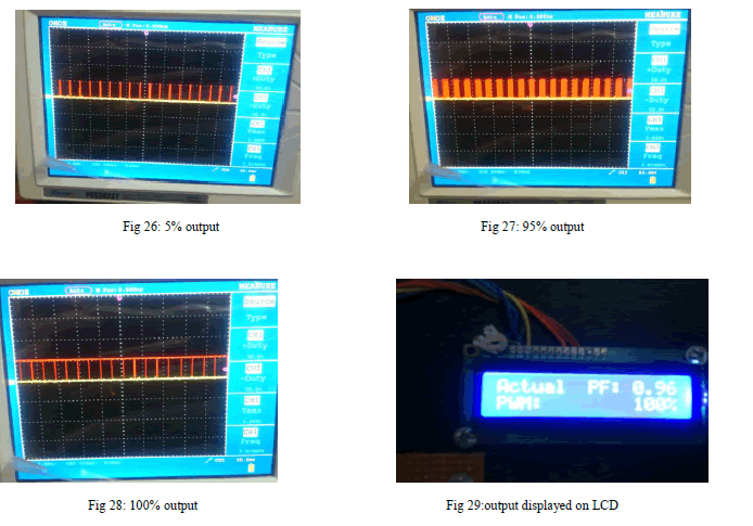 |
| We intend to produce a programmable power supply those whose output voltage can be varied as per user requirement. All this has been achieved using a simple low cost 8-bit microcontroller. Here we also provide an LCD display. As we can see we show the various parameters of PWM ratios as shown in above figures. As per the proposed work the above said power supply has been developed and a variable voltage from 0-50 volt DC on a 220 volt AC 15 watt load (15 watt bulb) has been achieved by employment of high frequency isolation transformer operating in buck-boost mode driven by microcontroller generated PWM signal. In the above said setup power factor ratios of 0.90-0.95 have been achieved as we can see in above figures. |
IX. CONCLUSION |
| The intended work has been done. We made a programmable power supply thatâÃâ¬ÃŸs output voltage can be varied as per the user requirement. As we can see the result has been achieved. In the result Power factor ratios 0.90-0.95 have been achieved. |
References |
|