ISSN ONLINE(2278-8875) PRINT (2320-3765)
ISSN ONLINE(2278-8875) PRINT (2320-3765)
Anna Joy1, Elizabeth Sebastian2, Reenu George3
|
| Related article at Pubmed, Scholar Google |
Visit for more related articles at International Journal of Advanced Research in Electrical, Electronics and Instrumentation Engineering
This paper presents a step up and step down dc to dc converter based on the three state switching cell.It can be used for high power applications.The circuit consists of two switches two diodes and two coupled inductors.This topology has 3 switching stages, thus the name given as three state switching cell. In this circuits only part of load power is transferred by the switches so switching stress is less and high power output up to 1.5 KW can be attained. Advantages of this topology are less size and volume of components, wide area of continuous conduction mode. Step up and step down converter have overlapping and non-overlapping modes. When duty ratio is less than 0.5, we can achieve non -overlapping and continuous conduction mode. Input voltage is taken as 200V, in buck converter 60V output and in boost converter 282V output is obtained at duty ratio 0.3.Simulations are done in SIMULINK/MATLAB.
Keywords |
| Buck Converter, Boost Converter, DC-DC Converters,Three State Switching Cell (3SSC) |
INTRODUCTION |
| Pulse-width modulated (PWM) converters are currentlyused in the majority of DC-DC conversion applications.Widespread applications of DC-DC converters include ups,variety of electronic systems, energysystems for telecommunications, systems for utilization ofsolar energy, DC motor drivers and energy systems forsatellites. Also DC-DC converters are often found as basicbuilding blocks for other types of power converters.This paper introduces a new family of PWM DC-DC non-isolated converters[1]. The new converters aregenerated using three-state commutation cells. Comprisingtwo active switches, two diodes and coupled inductors. The main advantages over the classical converters are lowconduction and commutation losses, and lowinput andoutput current ripple. Due to these features, the newconverters are suitable for high voltage and high current applications. Earlier days, conventional dc-dc converters are used single switch and hardswitching technique[2]. It have low power density and large switching losses. |
| To avoid abovelimitation, we uses soft switching, so it reduces overlap between voltage and current[6]. And also we can use snubber circuit for reducing switching losses.This circuit integrates the advantage of reduced voltage across the switches using three level commutation cell, and decreased switching losses obtained from a soft switching technique. By using interleaving technique in high current applications, output ripples can be reduced [3].This paper presents the method to obtain the three-stateswitching cells. The obtained cells are subsequently used tosynthesize a new family of DC-DC three-state switchingconverters.In the last few years, many converters based on the threestateswitching cell (3SSC) have been proposed. The cell can beobtained by the association of two 2-state PWMcells (2SSC)interconnected to a center tap autotransformer, from which novel converters can be derived. General advantages of 3SSC circuits over conventionaltopologies are, the inductor is designed fortwice the switching frequency, with consequent reduction of size and the current through the switches is half of the inputcurrent. In the 3SSC circuits, part of the input power is delivered to the load by thetransformer instead of the main switches, thus reducingconduction and commutation losses and lower cost switches can beused. Here we describe non overlapping mode and continuous conduction period. When duty ration is less than 0.5, non-overlapping mode can attained. |
| Evolution of 3SSC step up and step down converters can be described as,in earlier days classical dc-dc converters are used like buck, boost, buck –boost, cu’k etc. After these 2SSC circuits are invented, it has high power density and reduced size of reactive elements but switching losses are large so we uses soft switching techniques. Using zero voltage converter (ZVS) or zero current switching (ZCS) switching losses are eliminated but conduction losses are present. To avoid conduction losses, we can use multilevel converters. |
II. EVOLUTION OF 3SSC STEP UP AND STEP DOWN CONVERTER |
| 3SSC converters are actually evolved from conventional push pull converters[4]. In order to make 3SSC buck and boost circuits, we can replace high frequency transformer into coupled inductors.For this we can assume the turns ratio of central tap autotransformer is unity and ideal. Also connect the negative pole of the output voltage stage to the input negative pole. Thus we can achieve a converter with less switching losses. Characteristics of the 3SSC converters are[1]:Reduced size, and volume of magnetics, which aredesigned for twice the switching frequency analogouslyto the interleaved buck converter.The current stress through each main switch is equal to half of the total output current, allowing the use of semiconductorswith lower current ratings.Losses are distributed among the semiconductors, leading to better heat distribution and consequently more efficientuse of the heat sinks.Part of the input power, i.e., 50%, is directly transferred to the load through the diodes and the coupled inductors(autotransformers), and not through the main switches.As a consequence, conduction and switching losses are reduced.This is the main difference between the functionality of this approach and that of the interleaved bucktopology.The use of the 3SSC allows the parallel connection of switches and, therefore, inexpensive power devices anddrives can be used.Energy is transferred from the source to the load duringmost part of the switching period, which is a distinct characteristic of the proposed converter, since in other bucktypeconverters, it only occurs during half of the switchingperiod. As a consequence, reduction of current peaks andalso conduction losses are expected.The drive circuit of the main switches becomes lesscomplex because they are connected to the same referencenode, what does not occur in the interleaved buckconverter. |
| Several assumptions have to considered for the analysis of new 3SSC converters |
| 1) Converters are operates in steady state. |
| 2) Switching frequency is constant and PWM is employed to drive the switches. |
| 3) The gating signals of the switches are 1800 displaced. |
| 4) The turns ratio of the autotransformer is unity. |
| 5) The magnetizing current is much lower than the loadcurrent. |
| 6) All semiconductor and passive elements are ideal. |
III. 3SSC BUCK CONVERTER AND BOOST CONVERTERS |
| 3SSC buck and boost circuits consist of two diodes, two switches and two coupled inductors. Output voltage source consist of a snubber circuitsso Circuit cost is increased and reliability is affected by using active snubbers so we uses a passive lossless snubber it effectively restrict switching losses and electromagnetic interference (EMI) noise using no active components and no power dissipative components[1]. 3SSC converters are evolved from conventional push pull dc – dc converter. Push pull converter consists of two diodes,two switches but secondary side consists of a high frequency transformer,here dc-ac-dc conversion occurred. By assuming unity turns ratio for the central tap autotransformer. So we can replaced secondary windings by respective magnetizing inductance which are coupled and formed autotransformer. The negative terminal of the output stage represented by Vo, which was formerly connected to the central tap of the transformer, is then connected to the negative pole of the input voltage source to generate a boost topology. |
| Two modes of operations are described in 3SSC circuits in the basis of duty ratios. If duty ratio is larger than 0.5 overlapping mode is obtained, where two switches are conducted simultaneously. If duty ratio is less than 0.5 non overlapping mode is obtained, where two switches are operated in complementary. Only one switch is operated at an operating stage. The proposed circuit is an integration of interleaved technique and three state switching cell. |
 |
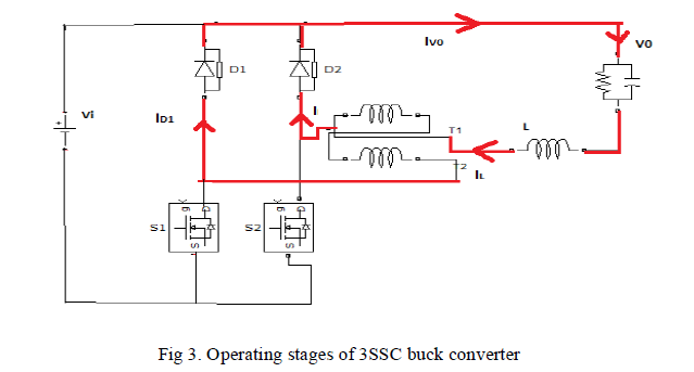 |
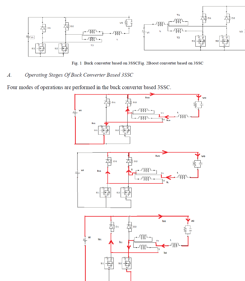
| MODE 1:Initially, switch S1 isturned ON, while switch S2 is turned OFF. The current throughthe inductor is divided in two parts. The first one flows through T2and D2 with energy being delivered to the load. The secondone flows through T2 and S1, current sharing is maintainedsince the number of turns for T1and T2 is the same. The currentthrough L increases linearly.Windings T1 and T2 have the sameimpedance, and the voltages across them are equal to half of theinput voltage Vi. This stage finishes when S1 is turned OFF [1]. |
| MODE2: Switch S1 is turned OFF, while switch S2 remains OFF. The voltage across inductor L is inverted. Diode D1 is forward biased while D2remains conducting. The energy stored in L during the previous stage is then transferred to the load. The current flows through T1T2, according to the given polarity, what causes the magnetic flow inthe core to be null. The current returns to the source analogouslyto the previous stage. This stage finishes when S2 is turned ON. |
| MODE3:This stage is similar to the first one, although switch S2 turned ON instead and S1 remains turned OFF. Diode D1keeps conducting and D2is reverse biased. |
| D1keeps conducting and D2is reverse biased. MODE4:This stage is similar to the second one, as the same equivalent circuit and operating conditions are valid in this case.[1] |
IV. SIMULATION RESULTS |
A. Simulink Model Of 3SSC Buck Converter |
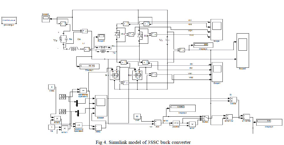
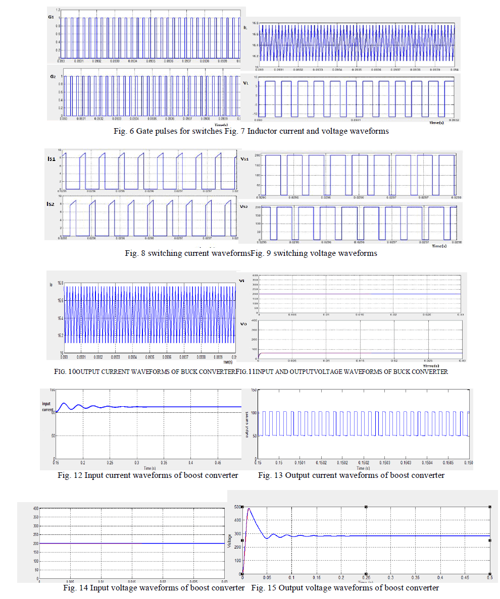
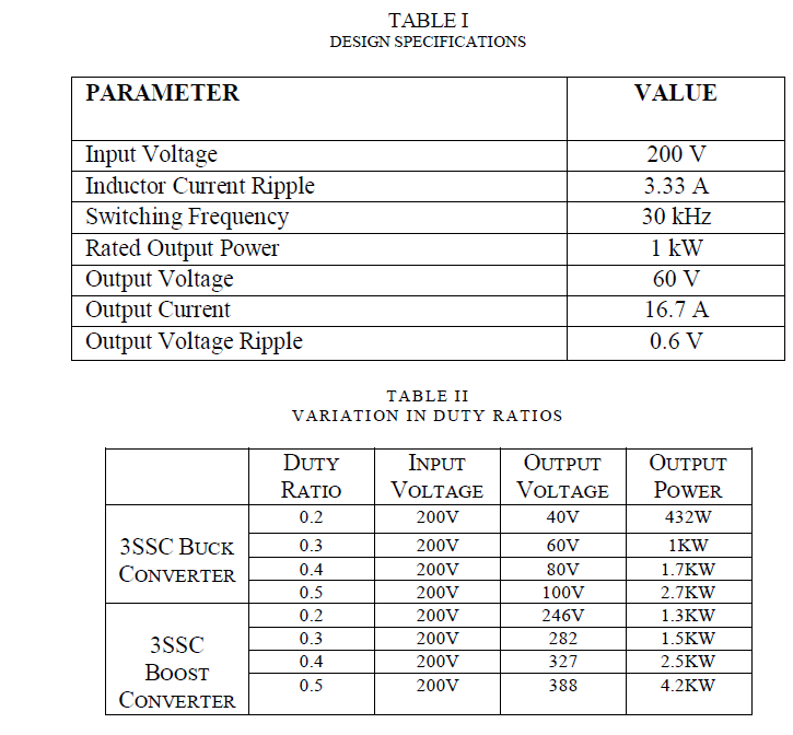
| For simulating 3SSC buck converter, we uses parameter values as R=3.6 ohm, C=14.72 e-6 F,L=120e-6 H. Input voltage is taken as 200V. For pulse generation we uses PWM generation and a controlled circuit is used to control output voltage.Output voltage is step downed and get 60V. Output current is 16 A. High output power 1KW is attained at duty ratio 0.3. As D varies output voltage also varies. D varies from 0.2 to 0.5. |
 |
B. Simulink Model Of 3SSC Buck Converter |
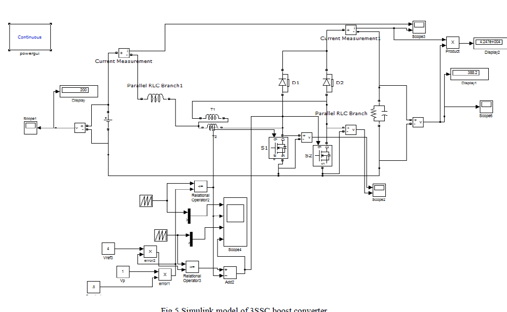
| For simulating 3SSC boost converter, we uses parameter values as R=3.6 ohm, C=14.72 e-6 F, L=120e-6 H. Input voltage is taken as 200V. For pulse generation we uses PWM generation and a controlled circuit is used to control output voltage. Output voltage is step upped and get 282V. Output current is 110 A.High output power 1.5KW is attained at duty ratio 0.3. As D varies output voltage also varies. D varies from 0.2 to 0.5. |
 |
| Observing the simulation results, gate pulses given to two switches are complementary in action. Analysing the inductor current, the switching frequency is half of the ripple current frequency, it leads to the reduction of magnetic elements. 200V input of buck converter is stepdowned to 60V and 200V of boost converter is step upped as 282V at duty ratio 0.3. |
 |
 |
V.CONCLUSION |
| Step up and step down converter based on three state switching cell for high application were simulated and results are noted. In step down converter an input voltage 200 V is given and we got 60 V as output at duty ratio 0.3.Output will vary according to D from0.2to 0.5. A controlled feedback is given to the buck converter. Buck converter based on 3SSC gives 1 KW output power. |
| In Step up converter an input voltage 200 V is given and got 282 V as output and 110 A current, 1.5KW power at D equal to 0.3. Duty ratio will vary from 0.2 to 0.5. After .5 duty ratio overlapping mode will occurred. Relationship between input-output voltages and duty ratio is observed as, in buck 3SSC converter V0/Vi=D and in boost 3SSC converter V0/Vi= 1/ (1-D).Simulations are done in SIMULINK/MATLAB R2010a. From the simulation results high output power is obtained and less amount of ripples were observed. . |
References |
|