Research & Reviews: Journal of Pure and Applied Physics
ISSN: 2320-2459
ISSN: 2320-2459
Department of Physics, Brahmdevdada Mane Institute of Technology, Solapur 413002, Maharashtra, India.
1Department of Physics, Shivaji University, Kolhapur, Maharashtra, India.
Received date: 26/05/2013 Revised date: 07/07/2013 Accepted date: 12/08/2013
Visit for more related articles at Research & Reviews: Journal of Pure and Applied Physics
Manganese Oxide thin films were prepared by pyrolytic decomposition of manganese acetate as a precursor solution onto the glass substrates. MnO2 thin films were deposited at three different temperatures namely 200, 250, 3000C. As deposited films were amorphous and porous having 200-300 nm thickness. The thin films were subsequently annealed at 5000C in the air for 2 hours. Structural, optical and electrical properties of MnO2 have been studied. Polycrystalline thin films with a cubic structure as evidenced from X-ray diffraction pattern. The electrical properties have been studied by means of electrical resistivity and thermo-electric (TEP) power measurements. The electrical resistivity studies were carried out using two-probe method. The TEP studies show that the films exhibits n-type conductivity. The optical absorption data were used to determine the (indirect ) band gap energy and is found to increase with increase in temperature
Spray pyrolysis technique (SPT), Manganese oxide thin films , Characterization.
Manganese oxide (MnO2) is a transition metal oxide. It is black in color and is used as an oxidizing agent, electr°Chemical catalysts [1], electrode materials [2,3]. MnO2 of different structures are deposited using several techniques such as thermal evaporation in vacuum [4], M°CVD [5] , sol-gel [6], spray pyrolysis [7]. Manganese oxide of different structure (MnO, Mn2O3, MnO2 and Mn3O4) is usually prepared by varying calcinations conditions of starting chemical precursor. They can also be prepared each other by varying the temperature and atmosphere (vacuum or air, oxygen, hydrogen etc.,) of the calcinations [5]. MnO2 is prepared in the form of thin films on glass substrate at various temperature by pneumatic spray pyrolysis technique and their structural, optical and electrical properties are studied. (Fig.1.1).
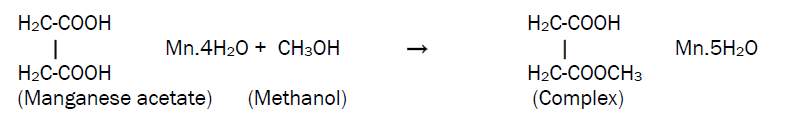
MnO2 thin films were grown on glass substrate using a typical spray pyrolysis technique. The spraying solution was prepared by dissolving appropriate quantity of precursor powder (manganese acetate) in methanol at room temperature according to the equation,
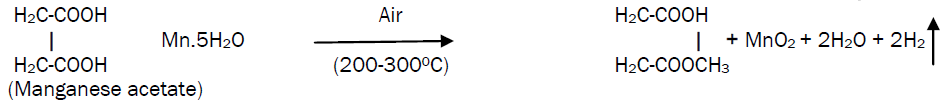
This solution is then atomized by compressed air at the pressure of 1 kg/cm2 on to the ultrasonically cleaned glass substrates. The sprayed droplets undergo solvent evaporation, solute condensation and thermal decomposition thereby resulting in the formation of manganese oxide thin film. The chemical reaction that takes place is given by the equation,
The substrate temperature was maintained at 200°C, 250 ºC and 300 ºC (± 2 ºC) through a therm°Couple as a sensor for temperature controller. The spray rate was kept constant at 12cc/min. The carrier gas flow rate was kept constant at 15 lit/min.

Figure 1.1: Spray pyrolysis technique
Structural analysis
The structural identification of MnO2 thin films deposited at various substrate temperatures from manganese acetate was carried out with an X-ray diffraction technique using an X-ray diffractometer (Philips PW1710) with CuKα radiations (λ=1.5406 Å). The diffraction patterns obtained for samples T1, T2, T3 are as shown in Fig. 1.2. The observed XRD patterns were compared with the JCPDS data [8]. The observed‘d’ values agree well with the standard‘d’ values and it was observed that all samples exhibit peaks corresponding to (104), (001), (311), (400) planes. The existence of shift in some peaks is due to internal strain existing in the crystalline due to the disproportionate array of the constituents [9]. The comparison with JCPDS data confirms the formation of Mn(OH)2 and MnO2. The standard and observed‘d’ values with corresponding (hkl) planes are listed in Table 1.

Table 1: X-ray diffraction data table.
The samples T1 prepared at lower temperature 200°C consists of Mn(OH)2 phase indicating an incomplete thermal decomposition of manganese acetate. The result is consistent with TGA analysis. It was also observed that the prominence of MnO2 phase was found to improve with an increase in deposition temperature. The films prepared at 250°C consists of mixed phase of Mn(OH)2 and λ- MnO2 and the films prepared at 300°C consists of λ- MnO2 phase.
Transmittance analysis
The films were further analyzed by optical absorption studies as well as transmittance study. The variation of optical absorption density ‘αt’ with the wavelength ‘λ’ for the films were carried in the wavelength range 400 to 800 nm with UV spectrometer. This optical data were further analyzed to calculate the band gap energy of MnO2 samples using the relation,
![]()
Where αo-constant, hν-photon energy, Eg - band gap energy
n= 1/2 for direct allowed transition
n = 2 for indirect allowed transition
Fig.1.3 shows the variation of (αhν)2 Vs (hν) for all samples and fig.1.4 shows the variation of (αhν)1/2 Vs (hν). The extrapolation of the straight line portions of the plots (αhν)2 Vs (hν) to zero absorption coefficient gives the values of direct band gap energy and extrapolation of the plots (αhν)1/2 Vs (hν) to gives the values of indirect band gap energy. It is found that indirect band gap of the samples increases with increase in temperature. The direct band gap energy for the samples at 250°C is minimum as compared to other samples. The transmittance increases with increase in substrate temperature as shown in fig. 1.5. Transmittance versus wavelength measurements were made using UV-VIS- NIR spectrophotometer (Hitachi model 330).
Thickness of the deposited films (T1-T3) was measured by using Taylor-Hobson’s Talystep instrument. The variation of film thickness with substrate temperature is as shown in fig. 1.6. From the graph it has been observed that the film thickness decreases continuously with an increase in substrate temperature. This behavior is attributed to the increase in evaporation rate of initial product before reaching to the substrate, with an increase in substrate temperature.
Electrical resistivity
In this study, two-probe method was used for dc electrical resistivity measurement in the temperature range 325 K to 550 K. The film was pastedwith silver to ensure ohmic contacts. A battery charge (30 V, 6A) was used to pass current through the film. Chromel- Alumel thermocouple was used to measure the temperature.
The fluctuations were observed in the electrical resistivity measurement of the as deposited manganese oxide thin films. Therefore, the deposited substrates were heated at 5000C for 2 hours and calculations were made. This induces maximum resistivity in 2500C sample amongst the three studied deposition temperatures. Electrical resistivity of all the films decreases with the increase in temperatures indicating the semiconductor nature of MnO2.
The room temperature electrical resistivity was calculated and found to be of the order of 105 Ω cm. The values of room temperature electrical resistivity for all the samples are summarized in Table.2 The temperature dependence of electrical resistivity from 325 K to 550 K for all the samples is as shown in fig. 1.7. The activation energy is calculated using the relation,
![]()
The Ea values are given in the Table.2. No systematic variation of Ea with substrate temperature was observed.
Thermo-electric Power (TEP) measurement

Table 2:Electrical and optical properties.
Thermo-electric Power is the ratio of thermally generated emf to the temperature difference across the semiconductor. It gives the information about concentration of charge carriers and the mechanism of electrical conduction. The emf was measured for all samples as a function of temperature in the temperature range 325 - 550 K. TEP for all samples were calculated from the slope of linear variations determined from experimental data listed in Table.2 and linear variations for all samples are as shown in fig. 1.8. As deposited manganese oxide thin films give fluctuations in TEP measurement due to amorphous and porous structure of the film. Sample deposited at 2500C after annealing at 5000C for 2 hours gives maximum TEP amongst all studied samples. Thermally generated electrons in the semiconductor migrates from hot to cold end and polarity of thermally generated voltage at hot end was positive for all samples, indicating that the films exhibits n-type conductivity.

Figure 1.2: The diffraction pattern obtained for samples T1, T2, and T3

Figure 1.3: Direct band gap energy.

Figure 1.4: Indirect band gap energy

Figure 1.5: Transmittance.

Figure 1.6: Thickness variation with temperature.

Figure 1.7: Resistivity of MnO2.

Figure 1.8: TEP of MnO2
MnO2 thin films were prepared using by spray pyrolysis technique. The structural analysis revealed the cubical nature of the film; it is also observed that the prominence of MnO2 phase was found to improve with an increase in deposition temperature. The indirect band gap energy of the material increases with increase in temperature. The electrical resistivity decreases with the increase in temperatures, indicating the semiconductor nature of deposited films. The thermo-electric power for deposited at 3000C has a lower value as compared to the other lower deposition temperature.
The authors would like express sincere thanks to all staff members of the physics department, Shivaji University, Kolhapur, Brahmdevdada Mane Institute of Technology, Solapur and University for their cooperation. The authors also acknowledge the help received from the staff of University science and Instrumentation Centre (USIC) and Common Facility Centre (CFC), Shivaji University, Kolhapur.