Research & Reviews: Journal of Material Sciences
ISSN:2321-6212
ISSN:2321-6212
Arthi. R*, S. Christopher, R. David Koilpillai
Department of Electrical Engineering, Indian Institute of Technology, Chennai, India
Received: 02-May-2023, Manuscript No. JOMS-23-97518; Editor assigned: 04-May-2023, PreQC No. JOMS-23-97518 (PQ); Reviewed: 18-May-2023, QC No. JOMS-23-97518; Revised: 25-May-2023, Manuscript No. JOMS-23-97518 (R); Published: 02-Jun-2023, DOI: 10.4172/2321-6212.11.3.003.
Citation: Arthi R, et al. Study and Analysis of a QFN Packaged 8-Bit Phase Shifter Design Using 65-nm CMOS Technology. RRJ Mater Sci. 2023;11:003.
Copyright: © 2023 Arthi R, et al. This is an open-access article distributed under the terms of the Creative Commons Attribution License, which permits unrestricted use, distribution, and reproduction in any medium, provided the original author and source are credited.
Visit for more related articles at Research & Reviews: Journal of Material Sciences
A digital 8-bit phase shifter using 65-nm CMOS technology for a band of 3 GHz -4 GHz is designed, fabricated and tested. This work is based on the switched line topology utilizing various combinations of filters with lumped components for achieving the desired performance. Though in the simulation the tolerances with respect to the requirement is much better when it comes to packaging it deteriorates due to uncertainties. Thus, this work aims to study the effect of bond wire on the phase shifter in a packaged condition. The insertion loss variation and the return losses are affected by the lead inductance but the phase performance remains more or less same as the design. The fabricated 8-bit phase shifter demonstrates an overall rms phase error less than 2.17â° over the band 3 GHz-4 GHz for all the 256 states. The insertion loss is increased by 4.76 dB for the reference state for the packaged chip and the variation in the insertion loss being ± 10 dB over all the states in the entire band. The measured input and output matching of the packaged chip are less than -4 dB and–6 dB over the entire band respectively
Complementary metal; Oxide semiconductor technology; Quad Flat no-lead; Beam forming; System on chip; Phased array antenna
The phase shifter is an essential component for beam steering in radar and present day communication applications. They are the critical component in any beam forming system. The beam pointing in a phased array highly depends on the phase shifter accuracy. Thus, a low cost and highly accurate, phase shifter design is much needed in the functioning of the phased array antenna. The optimum technology choice will result in the cost reduction with enhanced performance. The CMOS technology with high levels of integration of rf and digital circuits proves to be an optimum solution [1].
Phase shifters can be analog or digital based on the design topology. The analog phase shifters provides a fine resolution to position the beam accurately with additional Digital-to Analog (DAC) to provide the control voltages, which makes the system design complex and inaccurate for absolute phase values [2]. On the other hand digital phase shifters are formed using discrete phase shift blocks which are designed independently and cascaded to achieve the required absolute phase angles. Here the phase accuracy is defined by the least angle bit and requires only digital commands making the design simple without any feedback loop for its operation.
Figure 1 shows a simplified block diagram of a beam former SoC for radar where the phase shifter is placed in the common arm to both transmit and receive path, thus the design of a compact passive bidirectional phase shifter is necessary. The MMIC die designs after fabrication by the foundry have to be packaged with environmental protection for their commercial application. The packaged dies are preferred due to their compatibility and environmental susceptibility during assembly and operation without degrading the performance of the intrinsic chip [3].

Figure 1: Basic block diagram.
A 6 GHz-18 GHz, 5-bit reflection type phase shifter is designed in [4], exhibits an insertion loss of 9.4 dB ± 1.4 dB and an RMS phase error of 7° over the entire bandwidth. A Ku-band 5-bit digital phase shifter with 0.18-μm RFCMOS technology using n-MOSFET switches is given in [5], which exhibits an RMS phase error less than 12° from 9 GHz-15 GHz and an insertion loss less than 14.5 dB ± 0.5 dB with matching <14 dB at 12 GHz.
This design utilizes a parallel resonator for 90° phase shifter for exhibiting broad-band characteristics. A broadband L-band, 6 bit phase shifter design using 0.5-μm GaAs pHEMT technology with an area of 3.3 mm2 is designed in [5,6]. This design achieves an insertion loss of -3.8 dB ± 0.75 dB and an RMS phase error of less than 4° over the band of 1.4 GHz to 2.4 GHz. A 5–bit Digital phase shifter of 3 mm × 2 mm area using the GaAs pHEMT technology for a bandwidth of 2 GHz covering 34 GHz–36 GHz is designed in [7].
This design achieves an RMS phase error of less than 2.3°. The achieved insertion loss is 8 dB to 9.1 dB per bit and input matching <-14 dB over the band per state. A 6-bit switch type phase shifter fabricated using 0.15-μm GaAs pHEMT process for phased array application is designed in [8]. This work achieves a measured insertion loss of -9 dB ± 1.5 dB over the band of 11.5 GHz to 13 GHz. At 12 GHz an RMS phase error of 2.5° and RMS amplitude error of 0.65 dB is achieved. This design aims for a high precision at 12 GHz operation frequency. A 6-bit, X-band design using filter topologies to realize the 64 phase state with reduced insertion loss is designed in [9]. The design is fabricated in 0.25-μm GaAs process technology with the dimensions of 2.5 mm × 1.8 mm. The design achieves an RMS phase error <1.5° and RMS amplitude error less than 0.27 dB over the band of 8 GHz-12 GHz. At 10 GHz the insertion loss measured on wafer is 6.4 dB and 29 dBm input 1dB compression point is measured.
A 6-bit digital phase shifter for C band is designed in 0.7-μm G7S technology at GAETEC foundry [10]. The switching functionality is achieved using shunt inductors which resonates with the 0.7-μm MESFET device. An insertion loss of -6.5 dB ± 0.4 dB over the band of 5 GHz-6 GHz is achieved. The size of the design is 4.5 mm × 2 mm with the maximum RMS phase error of 12° over the band. This design is aimed for integration into T/R core chip. An accurate performance enhanced switched line topology based phase shifter in S-band using 65-nm CMOS technology is given in [11].
The RMS phase errors is <1° and 2° for the normalized bandwidth and an insertion loss <14 dB is achieved which is compensated using an on wafer designed LNA. A noise figure less than 2.4 dB achieved over the band. A Ka-band 4-bit digital phase shifter designed in GaAs, having a simulated insertion loss of -11 dB ± 1 dB with matching <8.8 dB and RMS phase error <4° over 36 GHz-38 GHz is in [12].
A 7 bit 2.4 GHz-4 GHz phase shifter, using switch-type phase shifting topology is designed in [13]. This design includes a compensation cell for phase and achieves a measured RMS phase error of 3.1° from 2.4 GHz–4 GHz and 1.5° from 2.8 GHz–3.7 GHz with averaged insertion loss and amplitude error being 4.5 dB-4.9 dB and 0.34 dB respectively.
Optimized switch design
The switched line phase shifter topology is considered in this work. Firstly, discrete blocks of phase values are designed and these are cascaded to realize the complete phase shifter. These blocks are then switched on and off in all possible digital combinations to achieve a phase shift of 360° required for beam scanning.
The primary component in this topology is the switches and the insertion loss from them has to be very minimal as they come in series to the RF signal path. In this design, the RF nMOS from technology pdk is used for the switching operations as they are easy to control since they do not require any negative control voltages. But in Si technology as the capacitive coupling of the switch with the substrate is predominant, it is difficult to make a good switch.
The switch insertion loss is primarily due to source-drain (Csd) junction capacitance, coupling capacitance with the substrate and the on-resistance [14]. The RF NMOS from tsmcN65 pdk comes with CMOS deep triple-well technology which reduces the noise coupling through it to the substrate and offers the possibility to fully isolate the NMOS devices.
In theory, this allows to bias the body terminal at a different potential from ground. In this work a typical value of the 10 KΩ and 20 KΩ resistor is connected at both gate and bulk terminals. A biasing resistor is connected at the gate to increase the isolation from the signal path. The topologies of switch designs studied are given in Figure 2. The variation in the insertion loss and phase over the band of 3 GHz- 4 GHz is as shown in Figures 3 and 4 respectively [11].

Figure 2: Switch design study.

Figure 3: Insertion loss variation over the band.


Figure 4: Insertion phase variation over the band.

For the values of R above 10 KΩ, the insertion loss is reduced and the variation in the insertion loss is also reduced to 0.35 ± 0.01 dB for the stated R values, as shown in Figure 2. The insertion angle found was around 6° without this resistor, whereas on introducing them, the insertion angle reduced to milli-degrees. Hence, choosing an optimum resistor value reduces the insertion losses and also the insertion phase with improving the system performance.
Phase shifter design
The least phase bits are implemented with simple inductor across the switch. In this work, the phase angles of 1.4°, 2.8°, 5.625° and 11.25° are realized using the topology shown in Figures 5 and 6. The control voltage Vc high corresponds to the reference state and Vc low corresponds to the phase shifting state. The difference between the on and off states gives to the required phase shift angle.

Figure 5: Least phase bit block design.

Figure 6: Mid phase bit block design.
The mid phase bit block of 22.5° and 45° phase values are realized with a combination of low-pass and band-pass network as shown in Figure 6. Whenever M1 and M2 are on with M3 off, the RF signal passes through the reference state and for the complementary control inputs the signal passes through the phase shifting state. The reference state equivalent is T-type band pass filter design with C2 being sum of Ca and off-capacitance of M3. The phase shift state equivalent is T-type low pass network with C1 equal the aggregate of Ca and off-capacitance of M2. The design equations for evaluating the equivalent circuit lumped components values are as given in [15].
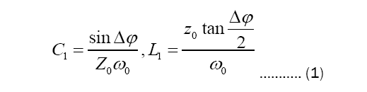
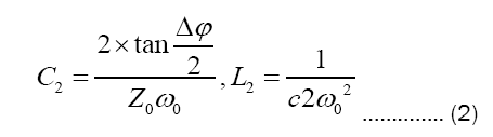
where Δφ is the required phase shift, Z0 is the terminal impedance and, ω0 is the design frequency.
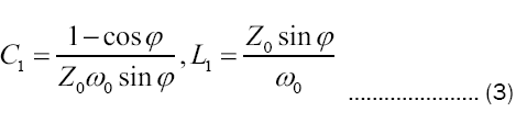
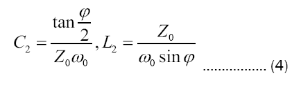
The higher phase bit blocks given by 90° and 180° are designed with a parallel implementation of high-pass and low-pass filter blocks such that when switched between the paths, their phase difference gives the required phase shift. The circuit implemented is as shown in Figure 7, and the corresponding design equations are as given below [16]:

Figure 7: High phase bit block design.
These blocks are now cascaded to give the complete 8-bit digital phase shifter. The layout diagram with the pads in tsmcN65 technology is as shown in Figure 8. The size of the phase shifter design considering the pads and seal ring is 1.68 mm × 0.8 mm. The die is then packaged with QFN 6 mm × 6 mm with 48 pads and gold wire bonds, as shown in Figure 9.

Figure 8: Layout of S band 8-bit phase shifter design.

Figure 9: The packaged chip containing the phase shifter die.
The phase shifter section is in the upper portion of the packaged chip as marked in Figure 9. In this work the average length of the bond wires for RF is 2.42 mm which is quite long. These bond wires give rise to lead wire inductance, in particular the RF terminals which affect the performance of the MMIC. Also, the conventional 180° spatial difference for RF input output ports are not considered due to some constraints and hence there will be additional coupling existing between the input and output. The lead parasitics, if not minimized has to be compensated in the design or accept the performance degradation. In this work, the plan is to study how much deterioration in the performance and which parameter get affected more due to bond wire.
The phase shifter being a passive design exhibits bi-directionality in operation. For the phase shifter, the input is at port 1 and output is at port 2, and the results are plotted accordingly.
RMS phase error
This parameter defines the precision of the phase shifter and hence the beam pointing accuracy. The simulated and measured RMS phase error over the entire band is as shown in Figure 10. The simulated RMS phase error of the die is less than 1.04° and the measured RMS phase error of the packaged chip is less than 2.17° over the entire band. Please note either the design or in the simulation the length of the bond wire and its effect was not considered.

Figure 10: RMS phase error with respect to the frequency.
Insertion loss
Insertion loss defines the loss/attenuation in the signal when it passes through the circuit. The simulated insertion loss for the die is shown in Figure 11. The measured insertion loss of the packaged chip for the entire states over the band is as shown in Figure 12. The simulated insertion loss varies from -14 dB ± 4 dB over the entire band whereas the measured value varies from -23 dB ± 10 dB. This proves that there is an average increase in both the insertion loss value as well as the spread over the band due to packaging. The simulated and measured insertion loss with all phase bits in off condition i.e. reference state is plotted as shown in Figure 13 for further studies.

Figure 11: Simulated insertion loss over the band.

Figure 12: Measured insertion loss over the band.

Figure 13: Simulated vs. Measured reference state insertion loss over the band.
The simulated design shows a nearly flat response for the given state over the band of operation whereas the measured data shows a variation of 4.5 dB over the band of 3 GHz to 4 GHz with an average increase in the insertion loss by 4.76 dB for the reference state.
Input return loss
The input matching of the simulated and measured design for the entire band is as shown in Figures 14 and 15 respectively. The simulated design has a matching better than -7 dB over the band and over the state whereas the measured matching is only better than just -4 dB over the band. Also as with increasing frequency the matching gets poor when measured which is inconsistent with the simulation. Hence this parameter has to be considered in the design stage. Since the phase shifter design in this work is planned to be the part of a transmit/receive module, the design can be matched with the previous stage component making it suitable for integration into a T/R core chip.

Figure 14: Simulated input return loss over the states and over the band.

Figure 15: Measured input return loss over the states and over the band.
Output return loss
The simulated and measured output return loss of the phase shifter over the entire band is as shown in Figures 16 and 17 respectively. In the design, the output matching is less than -10 dB over the entire band, whereas the hardware matching is significantly affected with values of less than -6 dB over the phase states and over the band.

Figure 16: Simulated output return loss over the states and over the band.

Figure 17: Measured output return over the states and over the band.
The bond wire that comes up in packaging has several effects and affects the performance of the design and hence this has to be considered in the design stage itself. Thus for an average length of 2.42 mm of bond wire in an S band design, the various parameters are studied in this section.
The design of a 8-bit switched line digital phase shifter with switch design optimization in tsmcN65 technology is discussed in details. The die is packaged using QFN 6 mm × 6 mm and the chip is tested. It is known that the bond wire effect has to be either compensated during the design or has to be reduced to minimal possible length. Generally rf inputs and outputs are 180° apart spatially for better performance. However there are situations which need the input and output to be nearby. In this work, the bond parasitics are uncompensated and also the spatial constraints are un-attempted to study their effects. For an average bond wire length of 2.42 mm the RMS phase error being a relative quantity is least affected with less than 2.17° over the entire band whereas the insertion loss and matching performances are most affected. The variation in the insertion loss over the band and states is ± 10 dB which indicates that a suitable compensation method needs to be brought in.