ISSN ONLINE(2278-8875) PRINT (2320-3765)
ISSN ONLINE(2278-8875) PRINT (2320-3765)
Piyush Sahu1, Vasant Acharya2
|
| Related article at Pubmed, Scholar Google |
Visit for more related articles at International Journal of Advanced Research in Electrical, Electronics and Instrumentation Engineering
Nowadays Off-shore wind farms are rising and promising alternative power sources. It requires HVDC transmission which has compact and reliable converter technology with large power capability. Multi-level Converter topology is a new and assuring converter for High Voltage Direct Current (HVDC) applications. To gain the compactness of the station the need for filters should be minimized. The Multilevel topology might address these aims. This paper introduces the research on modelling of VSC- HVDC System using Multi-level Converters, connecting two AC systems. This paper presents comparative analysis of a VSC-HVDC System using multi-level and two-level converter topology, to calculate THD. This paper briefly explains Multi-level VSC-HVDC system and its control system.
Keywords |
| MATLAB/ Simulink, Multi-level Converter, THD, Voltage source converter, VSC- HVDC. |
INTRODUCTION |
| High Voltage Direct Current (HVDC) technology has been in execution since 1954 and has been gaining in importance within the existing transmission system due to its advantages compared to AC transmission. The LCC based HVDC system is a mature technology which is primarily used for bulk power transmission over long distances but it has certain constraints such as the requirement of fairly strong AC networks to which it is connected and reactive power demand requirement by the converters. With the development of power electronics and the high switching frequency of PWM, VSC based HVDC transmission system has taken on some fantabulous advantages such as high controllability and potential to be connected to very weak ac systems. |
| The Voltage Source Converter (VSC) based HVDC system is a relatively new technology for low and medium power transmission which can be connected to weak or even passive AC networks and is capable of supplying or absorbing reactive power according to the system operating conditions. The converter which uses the voltage parameters as an input of it is called VSC. The main switching component of the VSC is a high-power high-frequency static switch (GTO, IGBT or MOSFET). The high-power high-frequency static switches, which were previously used for motor drives has to turn ON and turn OFF at any desired instance makes it a very attractive technology for various power system applications. The new VSC based HVDC system also known as âÃâ¬Ãâ¢HVDC LightâÃâ¬Ãâ and âÃâ¬Ãâ¢HVDC PlusâÃâ¬Ãâ by leading venders, has been applied in several occasions such as the connection of offshore wind farms or offshore oil & gas drilling platforms or solar farms into the mainland transmission network and power supply to isolated remote loads. |
| The new Voltage Source Converter based High Voltage DC transmission technology has some advantages over the conventional LCC based HVDC [5]:- |
| It is very easy to make multi terminal connections. |
| In addition, it has the option to control its terminal bus voltages in place of reactive powers; |
| The costs for filtering of harmonics may be significantly reduced if suitable PWM techniques are used; |
| VSC-HVDC system can independently control active and reactive power flows at its terminals; |
| Construction and commissioning of a VSC-HVDC system takes less time than that for a traditional thyristor based HVDC system. |
| It has no chance of commutation failures in the converter. |
| It has ability to connect to weak networks or even dead networks. |
| Also it has faster response due to increased switching frequency. |
| Lesser environmental impact. |
| Dependency on renewable energy sources are raising with increasing energy demand and due to implementation of renewable energy power plants, HVDC is more relevant than ever. Offshore wind farms require HVDC transmission which has compact and reliable converter technology with large power capability. There are number of distinct Voltage Source Converter topologies suitable for the carrying out of a VSC based HVDC transmission system but Multi level converter topology is a new and promising converter for High Voltage Direct Current applications and also the need of the filters should be minimized so we can gain the compactness. The Multilevel topology might address these aims. There are several multilevel converter topologies given in the technical paper [16]. Recently Multilevel converters has become more popular in high power application with the promise of less harmonics and the possibility to function at lower switching frequencies than ordinary two-level inverters. |
MULTI-LEVEL VSC HVDC SYSTEM |
| Fig. 1 shows the block diagram of the Multilevel VSC-HVDC system. There are different selected VSC topologies suitable for carrying out of a VSC-HVDC system. Each topology is distinct from each other. The main topologies are the diode clamped or neutral point clamped (NPC) converter, the cascaded H-bridge (CHB) converters and the flying capacitor (FC) converter [3]. |
 |
| The VSC- HVDC converter station contains the transformer, an AC-filter, Phase reactor, Voltage Source Converter consist of IGBT valve bridge, the converter control system and DC capacitors. Every IGBT is connected with an anti parallel diode. The converter is an array of controlled solid state switches which connect the dc input voltage periodically, for pre-determined intervals, to the output to produce the ac output voltage. The solid state switches of switch array may be increase depending on the number of DC voltage levels to be produced at the ac output of each converter phase module. As the number of voltage levels increases, the approximation of an ac sinusoidal output is approached but also increasing expense and circuit complexity. |
| A 2-level phase module is the simplest switching arrangement capable of producing ac output from a dc source in the form of a simple square-wave. A three-phase 2-level converter topology is illustrated in left side of Fig- 2. Two-level converter has square-wave output voltage waveform so the 2-level converter is unable to facilitate direct control of the amplitude of its output voltage but it can be easier with the application of PWM. A triangular carrier wave at a frequency of 1350 Hz which is 27 times of fundamental frequency, use in Sinusoidal Pulse Width Modulation (SPWM). |
| A three phase 3-level converter topology is illustrated in right side of Fig-2. Neutral point clamped (NPC) converter is widely used topology. The converter has three dc terminals to connect to a centre-tapped dc source. A three-level neutral point clamped voltage source converter consists of two capacitors in series, in which the center-tap uses as the neutral. A NPCML Converter typically consists of (n-1) capacitors on the DC bus where n is the total number of levels (positive, negative and zero) in the output voltage. Each phase module of the three-level converter has four switching devices in series. Upper two switches and lower two switches creates two pairs which is called phase arm and midpoint of each pair is clamped by clamping diodes to the neutral through. Additional diodes connect to the centre-tap dc supply which is the zero reference potential. The output voltage Vo of the converter can be positive, negative or zero. Vo has positive magnitude when both upper valves are triggered while Vo has negative magnitude when both lower valves are triggered. Vo has zero output when the upper and lower middle valves, connecting the centre-tap of the dc supply are triggered [7]. If switching uses a fundamental frequency then the output obtained from the three-level converter is a quasi-square wave output. In NPCML Converter diodes limit the voltage stress on switching devices. |
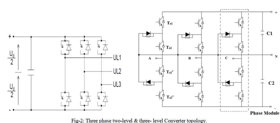 |
| Fig-2 shows a three phase three-level diode clamped converter. The switches for phase A are Ta1, Ta2, Ta1’, and Ta2’ and likewise for phase B and phase C. The DC bus voltage Vdc and the voltage across each capacitor is Vdc/2. The middle point of the two capacitors N is the neutral point. The principle of diode clamping is that by diode clamping we can extend DC voltages to desired magnitude and the voltages across the switching valves are limited by conduction time of the diodes connected according to the desired DC levels, this class of Multi-level converter is termed as diode clamped or neutral point clamped NPC [4]. |
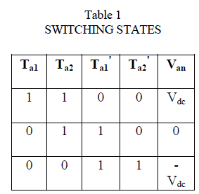 |
| Table 1 shows the output voltage levels and the corresponding switching states for the three-level NPCML Converter. The switches are arranged into 2 pairs (Ta1, Ta1’) and (Ta2, Ta2’). If switch Ta1 is turned on, the complementary switch Ta1’ must be off. Similar condition will apply for Ta2 and Ta2’. Two switches are ON at any point to select the desired level in the three-level NPCML Converter. The three-level converter output voltages for phase A are as follows: |
| 1. For an output voltage Van=0, switch Ta1 are turned off and switch Ta2 are turned on. |
| 2. For an output voltage Van =Vdc, all upper switches Ta1 and Ta2 are turned on. |
| 3. For an output voltage Van =- Vdc, all lower switches Ta1’ and Ta2’ are turned on. |
| The phase A output voltage Van has three states: Vdc, 0, and - Vdc. The gate signals for the chosen three-level DCMLI are developed using MATLAB-SIMULINK. |
CONTROL TECHNIQUE |
| Successful operation of the converter is depending on a well-functioning control system. Fig. 3 shows an overview of the VSC control system [15]. The controller 1 and controller 2 have identical designs and no communication between them. Both converters have two control modes: |
| Active and Reactive Power Control Mode |
| DC Voltage and Reactive Power Control Mode |
| The active power (or DC voltage) and the reactive power is controlled by the controlling of the parameter δ and the modulation index (m) respectively. The phase locked loop (PLL) is used to synchronize the controllers with the line voltage and calculate the phase synchronous angle Ãâè and the system frequency for the d-q transformations. |
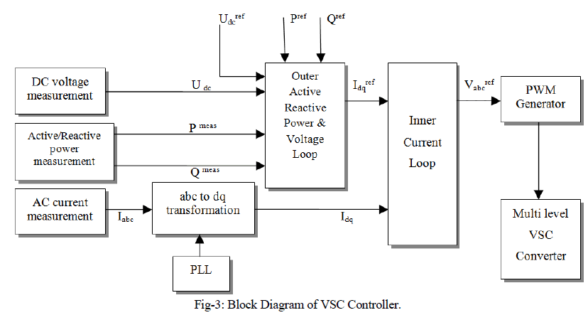 |
| The outer loop (active and reactive power and voltage loop) calculate the reference current vector (Idq ref) of the converter. The Outer Loop contains the Active Power Control, Reactive Power Control and DC Voltage Control blocks. The Reactive Power Control block combines a PI regulator with a feed forward control to increase the speed response and the AC Voltage control override block will interrupt the regulator and control it to maintain the AC voltage between the secure ranges in steady-state. The Active Power Control block is similar to the Reactive Power Control block. The DC Voltage control override block will interrupt the regulator and control it to maintain the DC voltage between the secure ranges especially during a perturbation in the AC system of the station controlling the DC voltage. The Active Power Control block is disabled then the DC Voltage Control regulator block is enabled. The block uses a PI regulator and its output is use for the reference current vector calculation. |
| The Inner Current Loop contains the AC Current Control block, tracks the reference current vector (Idq ref) with a feed forward scheme. A proportional integral feedback of the converter current is used to reduce the error in steady state. The output of the block is reference voltage vector. After that Inverse d-q and Inverse Clark transformation use to generate the three-phase voltage references modulating signals for PWM. |
| The instantaneous Active and Reactive Power of the converter on the valve side can be expressed as [15]: |
 |
| The above equation shows that the active and the reactive power are proportional to the d component and q component of the current respectively. According to this the active power (or DC voltage) and the reactive power (or AC bus voltage) is control by the current components ivd and ivq respectively. For each of the phases we can write: |
 |
| During unbalanced operation the expression for the voltage drop over the reactor (R + jωL ) are described as: |
 |
| Where X=p for positive sequence and X=n for negative sequence. Eq. (4) can be transformed to the α-β frame and then further transferred into the rotating d-q frame: |
 |
| The sequence voltages of the VSC are obtained from Eq. (5): |
 |
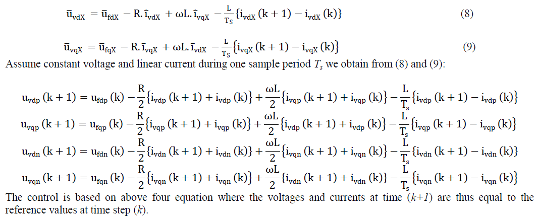
| The mean voltages for the sample period k to k+1 are derived from Eq. (6) and (7) by integrating from kTs to (k+1) Ts and dividing by Ts (where Ts is the sampling time). |
 |
SYSTEM CONFIGURATION |
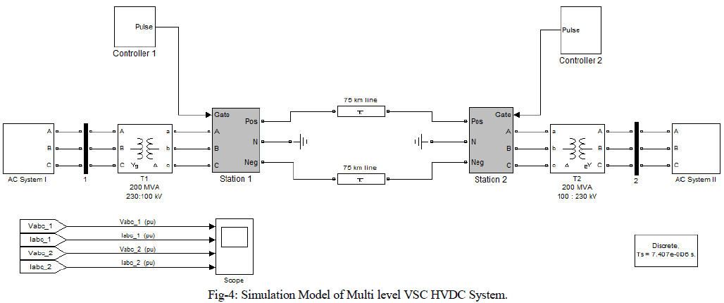
| A 200 MW 100 kV DC link is used to transmit power between two AC systems both are 230 kV, 2000 MVA, 50 Hz AC systems (AC system1 and AC system2). Fig-4 shows the simulation model of Multi-level VSC HVDC system. The VSC converters are modelled using ideal switching device IGBT because of its suitability for high-frequency switching. The rectifier (Station I) and the inverter (Station II) are Multi-level/ two level Neutral Point Clamped Voltage Source Converters using close IGBT/Diodes. In our model Multi-level converter has three-level. The Station I and the Station II are interconnected through a 75 km cable and two 8 mH smoothing reactors. A converter transformer (Yg/Δ) is used for voltage transformation. The winding arrangement blocks triplen harmonics. The VSC output voltage is in phase with respect to the AC system due to the phase reactor and the transformer leakage reactance. And also allow the control of active and reactive power output of the converter. The control system generates the three reference modulating signals that are the value of discrete 3-phase PWM Generator block of the Extras/Discrete Control Blocks library. The power system is discretized for a sample time 7.406e-6 s and the control system is discretized for a sample time 74.06e-6 s which is ten times of the carrier period. The converter uses Pulse Width Modulation (PWM) at 1350 Hz carrier frequency. In our case control modes for station I (rectifier side) and station II (inverter side) are P-Q mode and Ud-Q mode respectively. |
 |
SIMULATION RESULT |
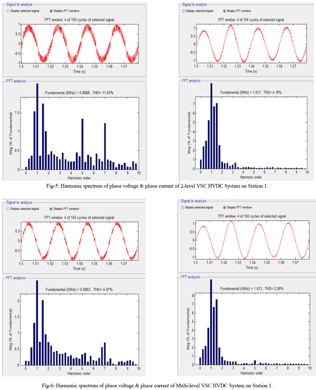
| The VSC HVDC Systems using sinusoidal pulse width modulation (SPWM) is simulated with the help of âÃâ¬Ãâ¢MATLAB 7.5.0âÃâ¬Ãâ. Simulation is carried out to observe the improvement in the phase voltage THD and phase current THD for VSC HVDC System as the converter level increases from 2-level to 3-level. Following quantities have been observed: |
| 1. Phase voltage waveforms. |
| 2. Phase current and Phase voltage waveform for VSC HVDC System on Station 1 and Station 2 for two level converter. |
| 3. Phase current and Phase voltage waveform for VSC HVDC System on Station 1and Station 2 for three level converter. |
 |
 |
CONCLUSIONS |
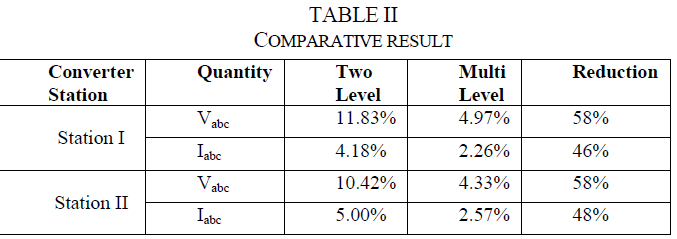
| In this paper simulation is perform for comparative study of VSC-HVDC System using Multi level and two level converter topology to calculate current and voltage harmonics. Multi level and two level converter topology was carried out using sinusoidal pulse width modulation (SPWM). The simulation results shows that the Multi level converter topology generate less harmonics. In Table II shows, voltage harmonics and current harmonics is reduced 58% and 46% respectively. That means voltage and current THD decrease when moves to three level converter topology from two level converter topology. |
References |
|