ISSN ONLINE(2278-8875) PRINT (2320-3765)
ISSN ONLINE(2278-8875) PRINT (2320-3765)
Devanshu1, Dr. R.K. Chauhan2
|
| Related article at Pubmed, Scholar Google |
Visit for more related articles at International Journal of Advanced Research in Electrical, Electronics and Instrumentation Engineering
A fundamental limitation of Silicon bipolar transistors is the inherent tradeoff between the dc current gain and the base resistance. One can overcome this limitation of Si bipolar transistors by introducing Germanium into the base material. In last several decades, silicon-germanium (SiGe) technology has come into the global electronics marketplace for its better noise performance in terms of the minimum noise figure, high speed performance, high cut-off frequency, low base emitter capacitance, low base resistance, high current density. As noise is a component in the transistors that degrades the performance of mobile wireless receivers, amplifiers and oscillators from meeting the essential requirements imposed on them while working at high frequencies in the GHz range. Small noise improvement on device level can have a large effect on the overall system performance. In this paper, an accurate noise model of SiGe HBT having 0.18 μm base width is being presented by observing the behaviour of its noise parameters, that is, minimum noise figure (NFmin), base transit time and a variety of analytical equations are being used to analyse and to compare the minimum noise figure NFmin as a function of the Ge concentration for rectangular or box type profile and the triangular profile of SiGe heterojunction bipolar transistor for the better performance. The results of simulated model have been presented based on VISUAL TCAD Simulator tool.
Keywords |
| SiGe HBT, NFmin, triangular profile, box or rectangular profile |
INTRODUCTION |
| Heterojunction is the crossing point occurs between the two layers of unlike semiconductor materials like Si and Ge. These semiconductor materials have uneven band gaps compared to that of the homo-junction. Among all the developments and the improvements through which BJTs have evolved, the most innovating and beneficial improvement is the substitution of the homo-junction emitter material by a wide band-gap material and in this way a heterojunction bipolar transistor (HBT) is formed and a higher base doping concentration to preserve the current gain can be used. In spite of the higher cost of the material, HBTs have gained popularity in digital and microwave applications first and foremost because of their better noise performance in terms of the minimum noise figure, high speed performance, high cut-off frequency, low base emitter capacitance, low base resistance, high current density and low noise figure. |
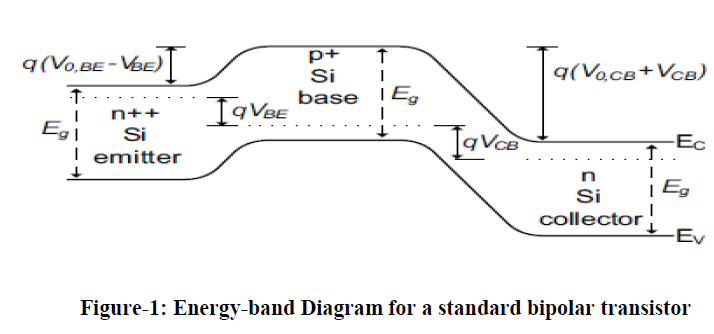
| A Silicon-Germanium (SiGe) HBT is produced by sandwiching a SiGe base between a Silicon emitter and a Silicon collector. The addition of Ge with Si in the base region, which leads to a strained SiGe base layer but the strain, is tolerable that shows that the layer thickness is lesser than a critical value and causes a band-gap to be reduced as compared to that in Si BJT. A fundamental limitation of Si bipolar transistors is inherent tradeoff between the dc current gain and the base resistance. This tradeoff occurs mainly because of the holes being injected back into the emitter and the electrons being injected into the base, that is, holes and electrons are responsible for potential barrier of the same height. Therefore, for a given thermal excitation, the electron and hole current both exerts the same thermal push and has to be optimized by giving the higher supply of mobile electrons in the emitter than that of mobile holes in the base. Hence, on increasing the current gain, ionized acceptor concentration reduces in the base, which in turn increases the base resistance. This behaviour can be well understood by the energy-band diagram for a standard Si bipolar transistor as shown in figure-1. |
 |
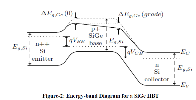
| As it turns out, one can overcome this limitation of Si bipolar transistors by introducing Ge into the base material. As the band-gap of Ge is 0.67 eV, which is significantly lower than the band-gap of silicon (which is 1.11 eV). Thus, by introducing a small amount of Ge to the base, it is possible to reduce the band-gap in the alloy considerably from that of pure silicon. Furthermore, by grading the Ge content as a function of depth in the base, the band-gap can be reduced along the base, resulting in reduction of base transit time. This behaviour can also be well understood by the energy-band diagram of a SiGe HBT indicating deviation from that of a pure silicon transistor. |
 |
| Introducing Ge into Si base has some consequences such as Ge has a larger lattice constant than that of Si and the energy band-gap of Ge is smaller than that of Si ( 0.66 eV Vs 1.12 eV). This SiGe alloy can be used to form the base layer of SiGe HBT. SiGe HBTs are proficient devices at nominal cost because of their compatibility with Si technology, widely used as compared with iii-v technology that offer superior velocity but at higher cost. For high frequency ac operation, bipolar transistors are repeatedly assessed by two figures of merit. The first figure of merit is known as the unity gain cut-off or transition frequency (fT) and the second figure of merit is known as the maximum oscillation frequency (fmax). Noise is one of the crucial properties that exists in all kinds of semiconductor materials and acts an important role in the performance of semiconductors. Noise is a component in the transistors that degrades the performance of mobile wireless receivers, amplifiers and oscillators from meeting the essential requirements imposed on them while working at high frequencies in the GHz range. Small noise improvement on device level can have a large effect on the overall system performance. In this paper, an accurate noise model of SiGe HBT having 0.18 μm base width is being presented by observing the behaviour of its noise parameters, that is, minimum noise figure (NFmin) , base transit time and a variety of analytical equations are being used to analyse and to compare the minimum noise figure NFmin as a function of the Ge concentration for rectangular or box type profile and the triangular profile of SiGe heterojunction bipolar transistor for the better performance. The results of simulated model have been presented based on VISUAL TCAD Simulator tool. |
II. NOISE MODELLING |
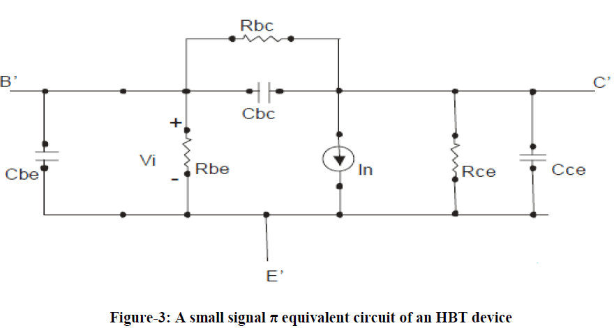
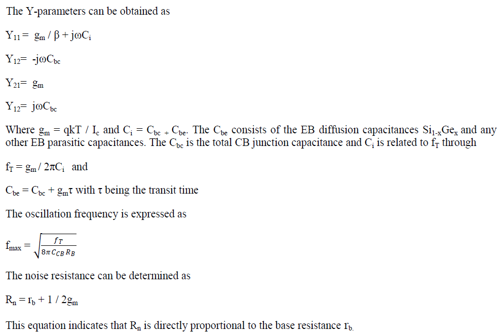
| The analytical expression for Rn, τb, NFmin are advantageous for gaining an additional intuitive insight for device optimization. A simple extraction method for determining the small signal π topology equivalent circuit of Silicon-Germanium (SiGe) heterojunction bipolar transistors (HBTs) has been developed. In order to express the validity of the model, first we obtain results by electrical simulation on VISUAL TCAD software and then compare these results with the results obtained through the analytical equations. |
 |
 |
 |
III. SIMULATION AND ANALYSIS |
| The noise figure and the base transit time of SiGe HBT are obtained for the various profiles, that is, for the box or rectangular type profile and triangular type profile. All the calculations are done through the simulation results obtained through Visual TCAD Simulator tool. In case of the rectangular profile, the Ge content remains the same in the base while in case of the triangular profile; the Ge content varies linearly from the emitter junction to the collector junction. |
A. The impact of Ge profile on the noise figure |
| In order to have a better reference to compare the model, we add a noise measurement in the device. As figure 4 shows the variation of minimum noise figure NFmin with the Ge concentration for the rectangular or box profile of SiGe HBT and it can be concluded that NFmin of SiGe HBT increases on increasing the Ge concentration. |
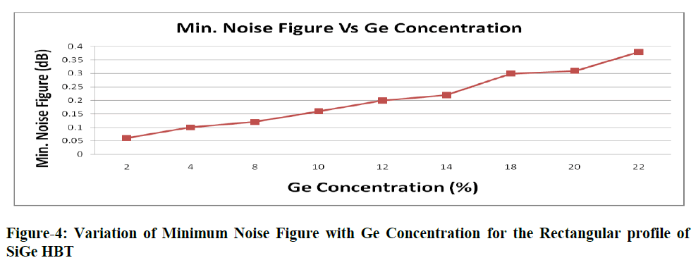 |
| This result matches with the analytical expression of NFmin which shows that NFmin increases monotonically with the Ge concentration. These calculations are based on the room temperature at 300 K. Figure-4 shows the analysis of simulated model for the rectangular profile of SiGe HBT which has noise figure of 0.325 dB (approx.) at 20% Ge concentration on VISUAL TCAD software. |
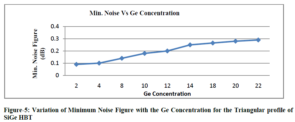 |
| Figure-5 shows the variation of minimum noise figure NFmin with the Ge concentration for the triangular profile of SiGe HBT and it can be concluded that NFmin of SiGe HBT increases on increasing the Ge concentration. These calculations are also based on the room temperature at 300 K. Figurme-5 shows the analysis of simulated model which has noise figure of 0.27 dB (approx.) at 20% Ge concentration on VISUAL TCAD software. |
B. The impact of Ge profile on Base Transit Time |
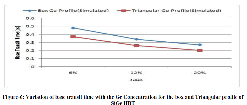
| It is shown in figure-6 that base transit time of SiGe HBT decreases on increasing the Ge concentration for both box profile as well as for triangular profile. It is also observed that the more optimal result is obtained from triangular profile, that is, base transit time in triangular profile of SiGe HBT is 0.20 ps (approx.) at 20% Ge concentration while in box type profile it is 0.28 ps (approx.) at 20% Ge concentration. |
 |
IV. CONCLUSION |
| In this work, we have focussed on the noise characterization of the device and noise analysis of two profiles as the rectangular profile and the triangular profile of SiGe HBTs that is implemented on VISUAL TCAD software and analyzed through a thorough method. The minimum noise-figure for these profiles are analysed and compared and it is found that the triangular profile is optimal one for having lower minimum noise-figure around 0.27 dB at 20% Ge concentration which is better than that of the rectangular or box type profile which has minimum noise-figure around 0.325 dB at 20% Ge concentration. Moreover Base transit time for box and triangular profile in SiGe HBTs is also obtained through the simulation and it is observed that the triangular profile gives better result as compared to box type profile. So we can say that triangular profile is optimal one in terms of noise- figure and base transit time as compared to the rectangular profile. Hence we can easily say that these simulation tools can be useful in noise optimization of the SiGe Heterojunction Bipolar Transistors. |
ACKNOWLEDGEMENT |
| The authors wish to thanks Prof. B. S. Rai, Vimal Mishra and Mr. Anand Pandey for their help and cooperation. |
References |
|