


 10 / 60

Page 52
conferenceseries
.com
Volume 6
Research & Reviews: Journal of Material Sciences
ISSN: 2321-6212
Advanced Materials 2018
September 04-06, 2018
September 04-06, 2018 | Zürich, Switzerland
21
st
International Conference on
Advanced Materials & Nanotechnology
Anew laser induced local material engineering to convert fromn-type to p-type nitride semiconductor
to fabricate high power vertical AlGaN/GaN devices on Si substrate
Yoshinobu Aoyagi
1
, Kurose N
1
, Matsumoto K
2
, Iwata T
2
and
Kamiya I
2
1
Ritsumeikan University, Japan
2
Toyota Technological Institute, Japan
Statement of the Problem:
The n-type aluminum gallium nitride (n-AlGaN) vertical field effect transistors (FETs) are
promising devices for future super high power FET electronics beyond Si, SiC and GaN devices. To realize n-AlGaN vertical
FETs with carrier blocking layer to concentrate the current flow into the vertical channel region, the local p-type AlGaN
formation is indispensable. So far, to realize this local p-type layer, crystal regrowth technique with lithography is carried out
but this process is complicated and reduces the crystal quality. To precede local carrier type conversion from n-type to p-type
without any crystal regrowth method, the carrier blocking layer can be easily produced without any crystal damages.
Methodology:
We used an excimer laser (193 nm) as an irradiation source for material engineering. The irradiation system has
a scanning system of the sample to control the irradiation area and an
in-situ
monitoring system to observe the material surface
during the laser irradiation. The material characteristics are observed using Hall effects, Kelvin probe and optical microscope
measurement.
Findings:
We found the insulating or n-type as grown Mg-doped GaN (Mg: GaN) was converted to p-type GaN (p-GaN)
under a proper laser irradiation condition only at the specific local area of the laser irradiation. The lateral resolution for
transition from the Mg: GaN to p-type was about 1 µm. The surface has no damage under the irradiation.
Conclusion & Significance:
A new technique has been established. This has achieved local activation of Mg: GaN to p-type
GaN using the laser irradiation co-operated with
in-situ
observations of the surface during the laser processing. Using this
method, local activation of carriers with the lateral resolution of about 1 µm is possible, thus establishing the potential for
fabricating local p-GaN carrier blocking layer and vertical high power devices without using any other fabrication techniques
such as crystal regrowth.
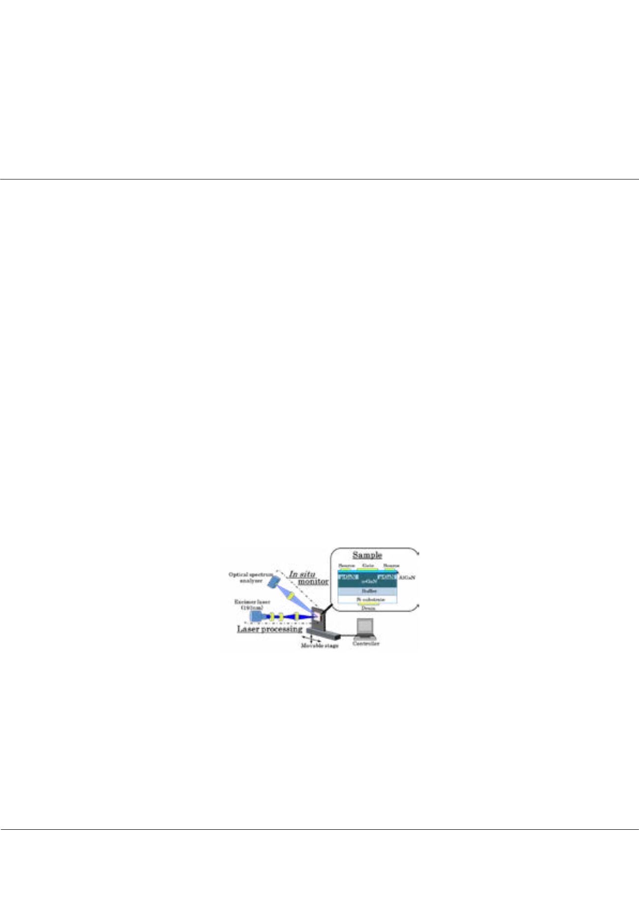
Figure: Experimental set up and sample to be converted locally from n-type to p-type GaN. The sample placed on the X–Y
stage was scanned using a controller. The PL and scattered light from the processing region of the GaN were monitored
in-situ
to feed the actual irradiation conditions back to the laser. The inset shows a schematic view of a vertical FET with a p-GaN
carrier-blocking layer which is locally converted from n-GaN by our method.
Recent Publications
1. Tanaka S, Iwai S and Aoyagi Y (1996) Self-assembling GaN quantum dots on Al
x
Ga1-
x
N surfaces using a surfactant.
Applied Physics Letters 69:4096-4098.
2. Tanaka S, TakeuchiMandAoyagi Y (2000) Anti-surfactant in III-nitride epitaxy -Quantumdot formation and dislocation
termination. Applied Physics Letters 39: L831-L834.
Yoshinobu Aoyagi et al., Res. Rev. J Mat. Sci. 2018, Volume 6
DOI: 10.4172/2321-6212-C3-020